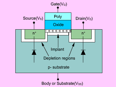
By implanting suitable impurities in the region between the source and the drain before depositing the insulating oxide and the gate, a channel can also be established. Thus the source and the drain are connected by a conducting channel even though the voltage between the gate and the source, namely VGS=0 (below the threshold voltage). To make the channel disappear, one has to apply a suitable negative voltage on the gate. As the channel in this device can be depleted of the carriers by applying a negative voltage Vtd say, such a device is called a depletion mode device. Figure 2.3 shows the arrangement in a depletion mode MOS device. For an n-type depletion mode device, penta-valent impurities like phosphorus is used.