If two nMOS switches are in series to produce "AND" function (which means here appearance of same voltage at nodes A and B by simultaneous conduction of both transistors) as shown in Figure 1.4(a), both of them should be closed (or ON) by connecting their gates to logic '1'. Similarly, to obtain a two-variable "AND" function by pMOS switches as shown in Figure 1.4(b), the gates should be fed by logic '0' signals. On the other hand, a two-input "OR" function (which means here appearance of same voltage in A and B by conduction of one or both of the transistors) is realized by placing two nMOS transistors (Figure 1.4(c)) or two pMOS transistors (Figure 1.4(d)) in parallel. The OR switch by nMOS transistors is closed if any one of the transistors is ON (that is, if any input is at logic '1'). At the same time, the OR function based on pMOS transistors is realized by placing logic '0' at either input.
1.2.3 NAND and NOR Gates
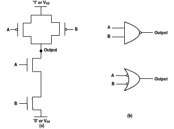
Figure 1.5 depicts CMOS implementation of a two-input NAND gate and its typical symbol. The pull-down sub-circuit is made of a series combination of two nMOS transistors. These are responsible for conducting logic '0' to the output node when both of the gates are at logic '1'.
Figure 1.5 : A two-input CMOS NAND gate and its symbol