The pull-up path on the other hand consists of a parallel combination of two pMOS transistors. If either of the is at logic `0', the output node assumes the value `1'. The two symbols shown in Figure 1.5(b) for a two-input NAND gate is due to the equivalence given by,
![]()
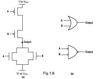
Figure 1.6 : A two-input CMOS NOR gate and its symbol
Figure 1.6 depicts CMOS implementation of a two-input NOR gate and its typical symbol. The pull-up sub-circuit is made of a series combination of two pMOS transistors. These are responsible for conducting logic `1' to the output node when both of the gates are at logic `0'.
The pull-down path on the other hand consists of a parallel combination of two nMOS transistors. If either of the inputs is at logic `1', the output node assumes the value `0'. The two symbols shown in Figure 1.6(b) for a two-input NOR gate is due to the equivalence
![]()