The truth table of the inverter shows a logic '1' output corresponding to a logic '0' in the input. This can be ensured by the p-transistor whose source is connected to a logic '1' source (VDD) and gate is provided a logic '0' stimulus. As in this condition, the n-transistor is OFF (that is, there is no current path between the output node and ground node) and the p-transistor channel is in the linear or resistive region of operation, one obtains perfect logic 1' at the output node. Similarly, a logic '0' output will result from a logic '1'input. The nMOS transistor connected in the bottom realizes this when its gate is given a logic '1' input and its source is connected to logic '0' or ground (VSS). In this case, the nMOS transistor channel acts like a wire resulting in logic '0' at the output while the pMOS transistor channel is simply devoid of any conductive channel.
The inverter can best be considered as the central part of digital designs. A thorough understanding of its operation and properties is required to design more complex structures like NAND and NOR gates, adders and multipliers.
1.2.2 Combinational Logic
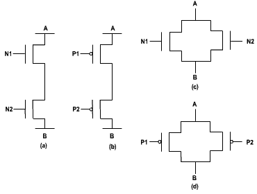
Combinational logic circuits, rather gates, perform Boolean operations on multiple input variables and determine the outputs as Boolean functions of the inputs. The basic two-input AND and OR functions can be realized by series and parallel combinations of nMOS and pMOS transistors as shown in Figure 1.4.