1.2.5 Memory : Latch and Register
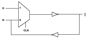
Semiconductor memory capable of storing large amount of information are essential to all digital systems. In its simplest form, a single-bit memory element can be realized as a latch or a register. A latch is a level-sensitive circuit for which the state of the output depends on the level of the clock signal. It passes the D input to the Q output when the clock signal is high (for a positive latch ) or when the clock is low (in case of a negative latch ). This latch is then said to be in transparent mode. During the low state of the clock, for a positive latch, the input data sampled at the falling edge of the clock is held stable at the output; the latch is now said to be in hold mode. The input should be stable for a short period around the falling edge of the clock to meet setup and hold requirements. Figure 1.9 depicts a positive level-sensitive latch implemented using a 2-input multiplexer and two inverters. It has a data input D, a clock input Clk, and two outputs Q and Q. The output Q follows the input D when Clk=`1'. When Clk=`0', the D input is ignored, and the state of output Q is retained. Similarly, a negative latch passes the D input to the Q output when the clock signal is low.