COMPOUND SEMICONDUCTOR FIELD-EFFECT TRANSISTORS(MESFETs)
- For device modeling suitable for Computer Aided Design (CAD), one
has to model the I-V characteristics for the entire range of drain-source
voltages, not only in the saturation regime.
- An empirical interpolation expression for the full, extrinsic MESFET
I-V characteristics was proposed using a hyperbolic tangent function
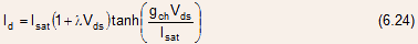
where is an empirical constant that accounts for the finite output conductance
in saturation, and
is an empirical constant that accounts for the finite output conductance
in saturation, and  is the extrinsic channel conductance of the linear region, given by

where is the intrinsic channel conductance at very low drain-source voltage,
and for a uniformly doped channel, from Eqn.(6.9):
is the intrinsic channel conductance at very low drain-source voltage,
and for a uniformly doped channel, from Eqn.(6.9):
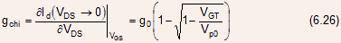
- The finite output conductance in saturation, described in terms
of the constant in
Eqn.(6.24), may be related to the short channel effects and to parasitic
currents in the substrate, such as space charge limited current.
- Hence, the output conductance may be greatly reduced by using a
heterojunctions buffer to prevent carrier injection into the substrate.
- The models discussed above are suitable for CAD of GaAs MESFETs
and GaAs MESFET circuits, however, some important second-order effects
are not included in these models, e.g.,
- subthreshold current and drain voltage induced shift in the
threshold voltage,
- deviation from the gradual channel approximation (GCA), which
may be especially important at the drain side of the channel,
- possible formation of a high field region (i.e., a dipole layer)
at the drain side of the channel,
- inclusion of diffusion and incomplete depletion at the boundary
between the depletion region and the conducting channel,
- ballistic or overshoot effects,
- effects of donor diffusion from the
 contact regions into the channel,
- effects of the passivating silicon nitride layer, and
- effects of traps.
- subthreshold current and drain voltage induced shift in the
threshold voltage,
- These factors may still be included indirectly by adjusting the model parameters such as mobility, saturation velocity, pinch-off voltage, etc., however, in a rigorous way, they can only be handled using numerical solutions, though for practical circuit simulators used in circuit design, analytical or very simple numerical models are still a necessity.
- These effects may strongly influence GaAs MESFET I-V characteristics.
- Backgating describes the effect of the substrate bias on the MESFET
characteristics, and sidegating refers to the effect of a nearby device
on the characteristics of a given MESFET.
- These effects are related to the finite depletion region, which
exists at the boundary between the MESFET active layer and the substrate.
- The width of this layer depends on the density of traps and on the position of the Fermi level in the substrate and may be found using an
- equivalent p-
junction" model, which predicts a certain dependence of the depletion
width and of the threshold voltage on the substrate bias.
- However, in practical circuits, sidegating usually plays a more
important role than backgating, and an accurate modeling of sidegating
effects is quite difficult.
- An empirical equation (similar to the body bias equation in MOSFETs)
is utilized in order to describe sidegating:

where is the threshold voltage unaffected by sidegating,
  is the source potential,
  is the potential causing the sidegating or backgating, and
  is a constant with a typical value of 0.1.
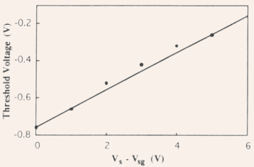
Fig.6.3 Experimental (symbols) and calculated (solid line) threshold voltage dependence on sidegating voltage.
- For sidegating,
is a function of the distance between the device and the sidegating
contact, with the experimental data presented in the literature predicting
that
is inversely proportional to this distance, and, usually, sidegating
becomes negligible only when this distance becomes quite large (at
least 30 to 40 m).
- The gate leakage current may play an important role in compound
semiconductor field effect transistors where the gate and the channel
are separated by the depletion region of the Schottky contact in GaAs
MESFETs.
- For enhancement mode compound semiconductor FETs, the gate current
can play a dominant role and may even affect the value of the "intrinsic"
drain-source current
 .
.
- The gate current is modeled by two equivalent Schottky diodes connected
from the gate to the source and from the gate to the drain.
- Using the well known diode equation, the total gate current can
be found as
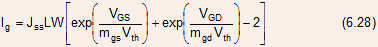
where Jss is the reverse saturation current density, calculated using either the thermionic or the thermionic-field emission theory, L and W are the gate length and gate width respectively, and
and  are the intrinsic gate-source and gate-drain voltages respectively,
 and
and  are the gate-source and gate-drain Schottky diode ideality factors
respectively, and
are the gate-source and gate-drain Schottky diode ideality factors
respectively, and  is the thermal voltage.
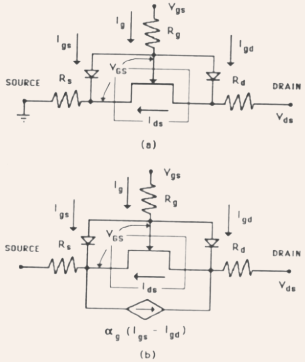
Fig.6.4 MESFET equivalent circuits: (a) conventional equivalent circuit, and (b) equivalent circuit that takes into account the effect of the gate current on the channel current.
- To a first order approximation, this simple model may be adequate
for a semi-quantitative description of the gate current in GaAs MESFETs.
- A more accurate description proposed introduced effective electron
temperatures at the source side and the drain side of the channel.
- The electron temperature at the source side of the channel is taken
to be close to the lattice temperature, i.e.,

 T, whereas the drain side electron temperature
  is assumed to increase with the drain-source voltage to reflect the
heating of the electrons in this part of the channel where the electric
field is large.
is assumed to increase with the drain-source voltage to reflect the
heating of the electrons in this part of the channel where the electric
field is large.
- This effect can easily be taken into account by modifying Eqn.(6.28)
to read

where and
and  are the reverse saturation current densities for the gate-source and
the gate-drain diodes respectively, and
are the reverse saturation current densities for the gate-source and
the gate-drain diodes respectively, and 
- In most GaAs MESFETs, the reverse gate saturation current is dependent
on the reverse bias, and this dependence can be described by:
where are the reverse diode conductances, and g is the reverse bias conduction
parameter.
are the reverse diode conductances, and g is the reverse bias conduction
parameter.
- These expressions reproduce MESFET leakage characteristics in excellent
agreement with the experimental data.
- Under forward bias, assuming thermionic emission mechanism,
- The equivalent circuit of Fig.6.4(b) takes into account the effect
of gate current on the channel current.
- Actually, the gate current is distributed along the channel, with
the largest current density taking place near the source side of the
channel, which leads to a redistribution of the electric field along
the channel, with an increase in the field near the source side of
the device, and an overall decrease in the drain current.
- This drop can even result in a negative differential resistance.
-
6.1 Determine the pinch-off voltage and the threshold voltage
for an n-channel GaAs MESFET with channel doping
6.2 Assume the device of Problem 6.1 has L = 2
6.3 Assuming
6.4 Consider a junction formed between an n-type GaAs MESFET channel doped at 2 x
6.5 Using the constant mobility model, calculate the MESFET and MOSFET transconductances in the saturation region for devices with a gate length of 5
6.6 Use the saturation velocity model to calculate the MESFET and MOSFET transconductances in the saturation region for devices with a gate length of 1
6.7 Choosing device data of your choice, calculate and plot the device threshold voltage as a function of the substrate doping. Discuss the advantages and disadvantages of a high substrate doping.
6.8 How would you scale the MESFET channel doping and thickness with the gate length? Explain.
6.9 What are the possible advantages and disadvantages of a MESFET with a lowly doped region near the drain?
6.10 A constant MESFET transconductance is very important for microwave applications since it allows one to reduce intermodulation distortion. Discuss how a MESFET doping profile can be tailored to obtain a region of the transfer characteristic with a nearly constant transconductance. For simplicity, assume complete velocity saturation in the channel.