COMPOUND SEMICONDUCTOR FIELD-EFFECT TRANSISTORS(MESFETs)
- Currently, compound semiconductor FETs play important role in the
electronics industry, e.g., GaAs FET amplifiers, oscillators, mixers,
switches, attenuators, modulators, and current limiters are widely
used, as well as high-speed ICs based on GaAs FETs and heterostructures
FETs (HFETs) have been developed.
- Basically obtained by combining elements from columns III and V
of the periodic table, e.g., GaAs, InP, InAs, InSb, AlAs, etc., having
a wide range of band gaps (both direct and indirect), lattice constants,
and other physical properties.
- Solid-state solutions are also possible, e.g., by varying the composition
x (from 0 to 1) continuously in the ternary compound
 ,
one may obtain a continuous change of the different material properties,
as the material changes from GaAs to AlAs.
,
one may obtain a continuous change of the different material properties,
as the material changes from GaAs to AlAs.
- GaAs is the most studied and understood compound semiconductor material,
and has proved indispensable for many device applications, e.g., ultra
high speed transistors to lasers and solar cells.
- Room temperature lattice constant of GaAs (5.653
 )
is very close to that of AlAs (5.661
) => the heterointerface between these two materials would have
very small density of interface states => ideal candidate for heterostructures
lasers.
)
is very close to that of AlAs (5.661
) => the heterointerface between these two materials would have
very small density of interface states => ideal candidate for heterostructures
lasers.
- Technological innovations, e.g., Molecular Beam Epitaxy (MBE) and
Metal Organic Chemical Vapor Deposition (MOCVD), allow growth of heterostructures
with very sharp and clean heterointerfaces, and have very precise
control over doping and composition profiles, typical resolution being
of the order of the atomic distances.
- Other compound semiconductors having applications in ultra high
speed submicron devices include
 ,
GaP, InP, AlN, etc.
,
GaP, InP, AlN, etc.
![]() Advantages of GaAs Systems
Advantages of GaAs Systems
- The room temperature electron mobility in GaAs (8500
 )
is much higher than that in Si (1250 ),
due to the lower electron effective mass in GaAs (0.067
)
is much higher than that in Si (1250 ),
due to the lower electron effective mass in GaAs (0.067 ,
where
is the rest mass for electrons) as compared to Si (0.98
for longitudinal effective mass and 0.19
for transverse effective mass).
,
where
is the rest mass for electrons) as compared to Si (0.98
for longitudinal effective mass and 0.19
for transverse effective mass).
- Also, under high electric fields, the light electrons experience
"ballistic transport" in GaAs for submicron devices, i.e.,
the electrons may move over a small distance without suffering any
collision (with either lattice vibration or lattice imperfections)
at all, and, thus, their instantaneous velocity can be far higher
than that in Si.
- Such ballistic transport is observed in devices having active device
dimensions of 0.1
 or less.
- For devices having active dimensions between 0.1
and 1.5,
electron velocity "overshoot" effects are important, which
may also result in boosting the electron velocity to considerably
higher levels than the stationary values.
- These effects are related to the finite time that it takes for an
electron to relax its energy.
- As shown in Fig.6.1, electrons very close to the injecting contact are moving ballistically and the electron velocity is proportional to time.
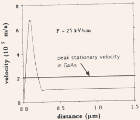
Fig.6.1 Electron velocity versus distance for electrons injected into
a region of constant electric field.
- Further from the contact, the velocity reaches a peak value, the
electron suffers a collision, and then the velocity decreases.
- Note: due to the overshoot effects, the peak value of the velocity
is much higher than the stationary value reached as the distance increases
further.
- In Si, ballistic and overshoot effects may also occur, however,
they are much less pronounced due to the larger electron effective
mass.
- Another important advantage of GaAs and InP devices is the availability
of semi-insulating substrates, which eliminate parasitic capacitances
related to junction isolation, and makes high-speed operation possible
and allows fabrication of micro strip lines with small losses (especially
important for applications in Microwave Monolithic Integrated Circuits
(MMICs)).
- Also, GaAs being a direct band gap semiconductor, it is highly suitable
for optoelectronic applications and makes possible a monolithic integration
of ultra high speed submicron transistors together with laser or LEDs
on the same chip for use in optical communication.
- These devices also have better radiation hardness since the direct
band gap results in high electron-hole recombination rates.
- New technologies, e.g., MBE and MOCVD, and availability of excellent heterostructures systems, e.g., AlGaAs/GaAs, GaInAs/InP, InGaAs/AlGaAs, etc., have opened up a plethora of new quantum devices, such as Heterostructure Field Effect Transistors (HFETs), Heterojunction Bipolar Transistors (HBTs), Hot Electron Transistors (HETs), Induced Base Transistors (IBTs), Permeable Base Transistors (PBTs), Vertical Ballistic Transistors (VBTs), Planar Doped Barrier Transistors (PDBTs), etc.
![]() Drawbacks of GaAs Systems
Drawbacks of GaAs Systems
- As compared to Si technology, GaAs technology is far more complex
and risky (since As is potentially a lethal substance).
- Also, since As have very high vapor pressure, they tend to evaporate
from the surface, making the crystal Ga rich => technological problem.
- Si has an excellent native oxide (
 ),
having reasonably high dielectric constant and excellent breakdown
strength.
),
having reasonably high dielectric constant and excellent breakdown
strength.
- On the other hand, the native oxide grown on GaAs (yielding both
 )
is nonstoichiometric, have very poor electronic properties, and creates
a very high density of interface states => GaAs MOSFETs still remain
a dream.
)
is nonstoichiometric, have very poor electronic properties, and creates
a very high density of interface states => GaAs MOSFETs still remain
a dream.
- Alternate choices: wide band gap AlGaAs and AlN may substitute as
an insulator, however, the performance is not encouraging.
- Recently,
on GaAs (oxidizing thin layers of Si deposited on GaAs by MBE) technology
holds some promise for developing GaAs MOSFETs sometime in the near
future.
- In any case, currently Schottky barrier MEtal Semiconductor Field Effect Transistors (MESFETs), Junction Field Effect Transistors (JFETs), and Heterostructure Field Effect Transistors (HFETs) are the most commonly used GaAs devices.
![]() Major Application Areas
Major Application Areas
- Mostly used for microwave and ultra high speed applications, where
their high speed properties are the most important, hence, scaling
down the device sizes in order to exploit the ballistic and/or overshoot
effects of the electron velocity are especially important.
- Use in the areas of
- optoelectronics (direct band gap)
- radiation-hard electronics (rapid EHP recombination due to direct
band gap)
- high-temperature electronics (large band gaps of most compound semiconductors
permit their use at high enough temperature, without leakage becoming
excessive)
- power devices (high breakdown field and the ability to speed-up their turn on by light)
![]() Modeling Aspects
Modeling Aspects
- Since this technology is much less developed than its Si counterpart,
reliable circuit and device modeling is especially important, and
development of accurate device models is a prerequisite for the commercialization
of compound semiconductor technology.
- Accurate device models have to be based on insight into the physics
of the devices, obtained from numerical simulations such as self-consistent
two-dimensional Monte Carlo modeling.
- Clearly, numerical device simulations are not directly applicable
to
- circuit design involving hundreds to thousands of transistors interacting
with each other and with other circuit elements,
- nor in device design where numerous dependencies of device characteristics
on the design parameters have to be optimized,
- nor in device characterization where the device and process parameters
must be extracted from experimental data.
- All these tasks require accurate analytical or semi-analytical device models, which must be based on physical device and material parameters, rather than using look-up tables and simple interpolations of the measured device characteristics, in order the provide the necessary feedback between the fabrication process and the device and circuit design.
![]() Basic MESFET Models
Basic MESFET Models
- GaAs MESFETs are widely used in both analog as well as digital
applications, with their microwave performance challenging that of
HFETs, and their IC integration scale rapidly approaching 100,000
transistors per chip and beyond.
- With thin, highly doped channels and low parasitic resistances, GaAs MESFETs can obtain high currents and transconductances.
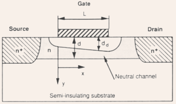
Fig. 6.2 Schematic representation of a MESFET.
- The gate electrode is deposited directly on the semiconductor and
forms a Schottky barrier contact with the conducting channel underneath,
between the source and drain ohmic contacts.
- The gate bias modulates the depletion region under the gate and,
thus, modulates the effective width of the neutral channel and thus
the current flow between source and drain.
- Note: the carriers under motion in the channel do not come under
close proximity of the interface due to the depletion region and,
thus, the problems related to interface traps are largely avoided.
- Also, since the forward voltage that can be applied to the gate
is limited by the built-in potential of the Schottky barrier, hence,
it is a drawback when the device is operated in enhancement (normally
off) logic, however, this limitation is less severe for low power
circuits operating with a low power supply voltage.
- Historically, MESFETs were discussed in early days in terms of the
Shockley model, where carrier velocity saturation effect was neglected,
and it was assumed that current saturation at high drain-source bias
took place as a result of the channel getting pinched-off at the drain
side of the channel.
- This model may be applicable for devices having very long channel
lengths, however, gives a poor description of modern day devices having
gate lengths of the order of 1 m or less.
- A deeper insight into MESFET device physics can be obtained from a detailed two-dimensional Monte Carlo simulation, however, simple analytical of semi-analytical models based on the device physics are still required for circuit simulators.
![]() The Shockley Model
The Shockley Model
- Consider first the gate region of a MESFET (intrinsic device) with
a uniform channel doping
 ,
a channel thickness d, and a built-in voltage
,
a channel thickness d, and a built-in voltage  for the gate contact.
- With a channel potential V(x) (relative to the intrinsic source)
and an intrinsic gate-source voltage
 ,
the depletion width
,
the depletion width .gif) can be expressed (using the gradual channel approximation [GCA]) as
can be expressed (using the gradual channel approximation [GCA]) as
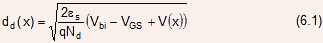
where is
the dielectric permittivity of the semiconductor and
is the built-in voltage of the source-channel junction.
is
the dielectric permittivity of the semiconductor and
is the built-in voltage of the source-channel junction.
- The threshold voltage
 corresponds to the gate-source voltage at which the depletion width
at zero drain-source bias (V = 0) equals the channel width, or, in
terms of Eq.(6.1)
corresponds to the gate-source voltage at which the depletion width
at zero drain-source bias (V = 0) equals the channel width, or, in
terms of Eq.(6.1)

where is referred to as the pinch-off voltage, and for a uniformly doped
channel, is given by
is referred to as the pinch-off voltage, and for a uniformly doped
channel, is given by
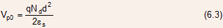
EXAMPLE 6.1: A GaAs (
SOLUTION: From Eqn.(6.3), the pinch-off voltage
The source channel junction is a high-low (
Therefore, from Eqn.(6.2), the threshold voltage is given by
- For >
, the channel is not fully depleted and a finite neutral region exists
in the channel, which allows a significant drain current to pass,
with magnitude increasing with an increase in .
- For <
,
the channel is fully depleted, and the drain current drops to a low
value, characteristic of the subthreshold region of operation.
- Note: from Eqn.(6.1), it is obvious that the depletion width under
the gate increases from source to drain when a positive drain-source
bias is applied.
- The depletion width at the drain side of the gate
.gif) ,
where L is the gate length, is obtained by replacing the channel potential
by the intrinsic drain-source voltage
,
where L is the gate length, is obtained by replacing the channel potential
by the intrinsic drain-source voltage  in Eqn.(6.1).
- In the absence of velocity saturation of carriers,
increases with increasing until
the channel is pinched-off, which occurs when =
d, corresponding to