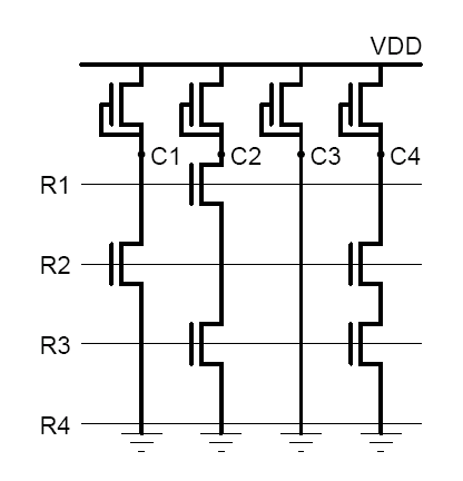
In this types of ROM array which is shown in Figure 31.31, each bit line consists of a depletion-load NAND gate, driven by some of the row signals, i.e. the word lines. In normal operation, all word lines are held at the logic HIGH voltage level except for the selected line, which is pulled down to logic LOW level. If a transistor exists at the cross point of a column and the selected row, that transistor is turned off and column voltage is pulled HIGH by the load device. On the other hand, if no transistor exists (shorted) at that particular cross point, the column voltage is pulled LOW by the other nMOS transistors in the multi-input NAND structure. Thus, a logic "1"-bit is stored by the presence of a transistor that can be deactivated, while a logic "0"-bit is stored by a shorted or normally ON transistor at the cross point.
Fig 31.31: NAND-based ROM
As in the NOR ROM case, the NAND-based ROM array can be fabricated initially with a transistor connection present at every row-column intersection. A "0"-bit is then stored by lowering the threshold voltage of the corresponding nMOS transistor at the cross point through a channel implant, so that the transistor remains ON regardless of the gate voltage. The availability of this process step is also the reason why depletion-type nMOS load transistors are used instead of pMOS loads.
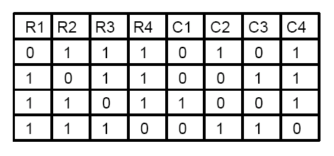
Fig 31.32: Truth table for Fig 31.31
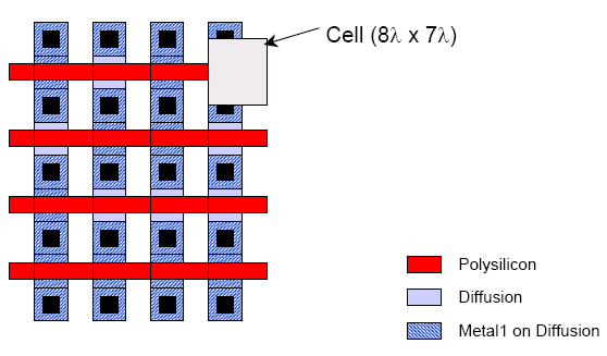
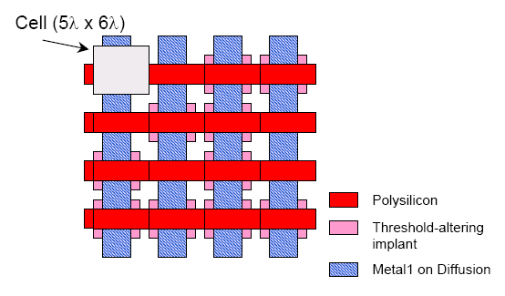
Figures 31.33 and 31.34 show two different types of layout implementations of NAND ROM array. In the implant-mask NAND ROM array, vertical columns of n-type diffusion intersect at regular intervals with horizontal rows of polysilicon, which results in an nMOS transistor at each intersection point. The transistor with threshold voltage implant operate as normally-ON depletion devices, thereby providing a continuous current path regardless of the gate voltage level. Since this structure has no contacts embedded in the array, it is much more compact than the NOR ROM array. However, the access time is usually slower than the NOR ROM, due to multiple series-connected nMOS transistor in each column.
Fig 31.33: Programming using the Metal-1 Layer Only