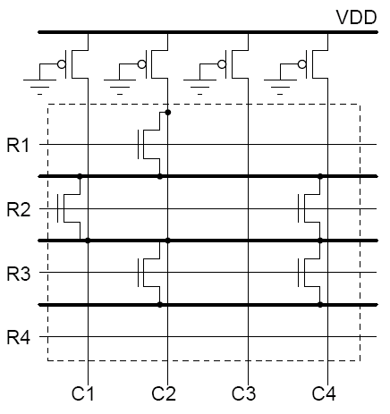
There are two different ways to implement MOS ROM arrays. Consider the first 4-bit X 4-bit memory array as shown in Figure 31.21. Here, each column consists of a pseudo-nMOS NOR gate driven by some of the row signals, i.e., the word line.
Fig 31.21: NOR-based ROM array
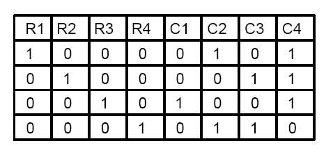
As we know, only one word line is activated at a time by raising tis voltage to VDD, while all other rows are held at a low votlage level. If an active transistor exists at the cross point of a column and the selected row, the column voltage is pulled down to the logic LOW level by that transistor. If no active transistor exists at the cross point, the column voltage is pulled HIGH by the pMOS load device. Thus, a logic "1"-bit is stored as the absence of an active transistor, while a logic "0"-bit is stored as the presence of an active transistor at the cross point. The truth table is shown in Figure 31.22.
Fig 31.22: Truth Table for Figure 31.21
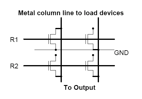
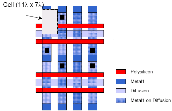
In an actual ROM layout, the array can be initially manufactured with nMOS transistors at every row-column intersection. The "1"-bit are then realized by omitting the drain or source connection, or the gate electrode of the corresponding nMOS transistors in the final metallization step. Figure 31.23 shows nMOS transistors in a NOR ROM array, forming the intersection of two metal lines and two polysilicon word lines. To save silicon area, the transistors in every two rows are arranged to share a common ground line, also routed in n-type diffusion. To store a "0"-bit at a particular address location, the drain diffusion of the corresponding transistor must be connected to the metal bit line via a metal-to-diffusion contact. Omission of this contact, on the other hand, results in stored "1"-bit.
Fig 31.23: Metal column line to load devices
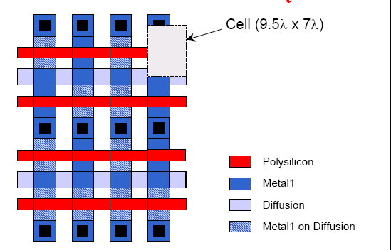
The layout of the ROM array is shown below in Figure 31.24.
Fig 31.24: Programming using the Active Layer Only
Figure 31.25 shows a different type of NOR ROM layout implementation which is based on deactivation of the nMOS transistor by raising their threshold voltage through channel implants. In this case, all nMOS transistors are alreadly connected to the column lines: therefore, storing a "1"-bit at a particular location by omitting the corresponding the drain contact is not possible. Instead, the nMOS transistor corresponding to the stored "1"-bit can be deactivated, i.e. permanently turned off, by raising its threshold voltage above the level through a selective channel implant during fabrication.
Fig 31.25: Programming using the Contact Layer Only