Here, we are going to introduce the concepts on which logical effort is based. Logical
effort as introduced by Sutherland et al is just a formalized representation of these
concepts.
The propagation delay of a MOS transistor depends on the capacitance of the transistor.
So, as the width W is increased capacitance increases and so does the propagation delay.
Let us say that when Cin, the input capacitance of a gate (say inverter) is equal to CL, the
load capacitance, then the propagation delay of the gate is
. If CL is not is equal Cin, then
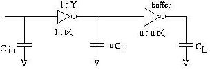
Now let us see that if we can introduce a buffer then can we reduce the propagation delay
of the gate (see figure 21.11).
Here, the input capacitance of 1st gate is Cin and the load capacitance is Cl. The input
capacitance of 2nd gate, which is also load to the 1st, is uCin.Consider, . Now,
Fig 21.11: A circuit for propagation delay calculation
Now, let us find out the optimum CL for which introducing a buffer will provide
Cin performance improvement. For this we use
the following: Solving this differential equation leads to the following result,
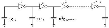
From the above result, we observe that a buffer will yield better results for Y > 4. Here the input capacitance of first gate is Cin,
that of 2nd is uCin, hat of next is and so
on and for the last one the input capacitance is .
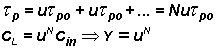
We have,
Fig 21.12: A circuit of high order for propagation delay calculation
taking lnu=1 and Y=1000. Therefore, with 7 stages we can drive a load capacitance 1000 times theinput capacitance.
Such cases arise when we have situations where we have to drive, lets say, a motor. Then
Y> 1000 and large currents have to be delivered.
In such cases where load current is to be provided outside chip then buffer should be put
very close to the output pad to avoid adding line capacitance.