Module 6 : LIGHT EMITTING DIODE (LED)
Lecture : LED - I
 

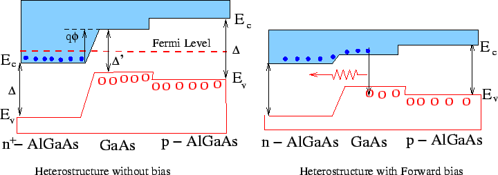
Recombination of electrons and holes also takes place non-radiatively, which reduce output of the device. The fraction of the electrons that are injected into the depletion layer which results in photons getting produced is called the internal quantum efficiency of the LED, usually denoted by $ \eta$. If $ N$is the number of electrons injected into the depletion layer every second, the power output of the device is given by
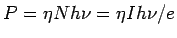
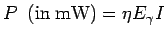
$\displaystyle P = \eta Nh\nu = \eta Ih\nu/e$

where $ I$is the forward current and $ e$the electronic charge. If the energy of the photon is measured in electron volts, the current in milli-amperes, the above expression for power output becomes

$\displaystyle P\ \ {\rm (in\ mW)}= \eta E_{\gamma} I$

  Example 1 :
  A GaAs LED radiates at 900 nm. If the forward current in the LED is 20 mA, calculate the power output, assuming an internal quantum efficiency of 2%.
  Solution :
 

The energy of the photon (in eV) is

$\displaystyle \frac{hc}{e\lambda} = \frac{6.62\times 10^{34}\times 3\times 10^{8}}{1.6\times 10^{-19}\times  9\times 10^{-7}} = 1.38$

Thus the power output is $ P = 0.02\times 1.38\times 20 = 0.55$mW.

1.2.1 Double Heterojunctions :
  One of the ways in which light output in LEDs is increased is to use heterojunction rather than homojunction described above. A heterojunction is a junction of two materials of different band gaps.

\includegraphics{led7.eps}

In the double heterostructure shown above a layer of p - tye GaAs is sandwitched between a heavily doped n-type AlGaAs and a lightly doped p-type AlGaAs. The band gap of AlGaAs is 1.92 eV while that of GaAs is 1.42 eV. Thus electrons to the left of the GaAs layer find a potential barrier. In the absence of a bias, the Fermi energy is uniform. When a forward bias is applied, the hight of the barrier is reduced at both the junctions. The electrons from the left can climb up the reduced barrier and enter the GaAs layer. However, they remain confined to this layer as in going over to the layer on the right they find a further potential barrier. The electrons and holes (which are already existing in the confining layer) combine and emit radiation. The emitted photon is no reabsorbed by the material as the band gap on either side of the confining layer is large. They escape to the surface.