As the concentration of holes is higher on the p-side, holes diffuse towards right and enter the n-side combining with the majority carriers, viz. electrons. The n- side gets depleted of electrons and develop net positive charge. In a like manner, electrons diffusing to the left create negative charges. Thus the region near junction develop an electric field which stop further diffusion of charges. This region, which is free of carriers, is called depletion region or space charge layer.
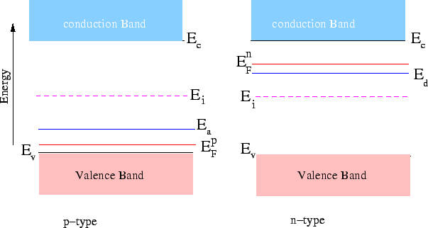
In the band picture, the Fermi level  for the p-type lies closer to the top of the valence band than the acceptor level and the Fermi level for the p-type lies closer to the top of the valence band than the acceptor level and the Fermi level  for the n-type lies closer to the bottom of the conduction band than the donor level. It may be recalled that if the effective masses of the electrons and holes are taken to be equal, the intrinsic Fermi level lies in the middle of the gap. for the n-type lies closer to the bottom of the conduction band than the donor level. It may be recalled that if the effective masses of the electrons and holes are taken to be equal, the intrinsic Fermi level lies in the middle of the gap.
When a junction is made of a p- type and an n-type material, the Fermi level on the two sides are not aligned. Since the Fermi level for a system in equilibrium must be uniform, band bending takes place. In the absence of a bias, the bottom of the conduction band on the n-side lies lower than that on the p-side. This prevents net diffusion as the electrons have to overcome a potential barrier  . . |