Experimental results:
To measure the effects of spin-transfer torques experimentally, the device should be fabricated such that current flow is restricted to a small diameter:
1. The amount of current needed to excite magnetic excitations using spin transfer mechanism scales with the total magnetic moment of the free layer. This is achievable by making the free layer a few nm thick and a few hundreds of nm in diameter.
2. It is necessary to utilize small devices in order that the effects of spin transfer dominate over the effects of the magnetic field that is generated by the current.
3. Spin-transfer effects are easiest to interpret in devices small enough that the free-layer moment moves as a single domain, which also typically requires devices close to the 100-nm scale.
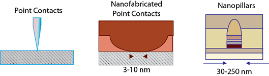
Figure 23.1: Typical sample geometries used for studying spin-transfer torques.
Figure 23.1 shows different types of magnetic-multilayer devices to demonstrate spin-transfer effects. One is the mechanical point contact device, in which a magnetic multilayer is contacted by a sharp metal tip to form a contact region on the scale of few tens of nm. Lithographically fabricated point contact devices have also been used to produce a similar device geometry. In both varieties of point contacts, excitations of the magnetic layers can be generated within a nanoscale region in the vicinity of the contact. Since the excited region is connected to a macroscopic magnetic film in the point contacts, a large current density (> 109 A/cm2) is required. The third variety of device is the multilayer nanopillar, in which the free magnetic layer is patterned to a small cross-section so that it is not exchange-coupled to a larger film. Figure 23.2 depicts the switching (hysteresis) of the free layer in a Py (2 nm)/ Cu (6 nm)/ Py (20 nm) spin-valve nanopillar at 4.2 K driven by a magnetic field applied in the plane of the sample along the easy axis (Figure 23.2a) and by a current (Figure 23.2b). The loops in Figure 23.2a shows a simple switching of the free-layer moment between parallel (P) and antiparallel (AP) alignment with the fixed layer, and provides a determination of the resistance values corresponding to these two states. In Figure 23.2b, a magnetic field is applied to cancel this dipole coupling between the magnetic layers, leaving the free-layer subject to zero net magnetic field. Figure 23.2b shows that the current can also be used to switch the magnets between the same two (P and AP) states.