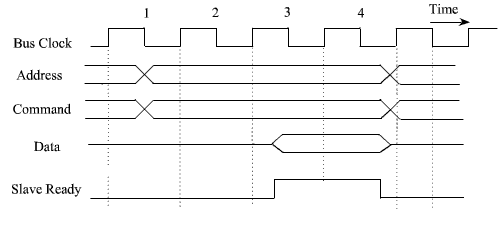
An instance of this scheme is shown in the Figure 7.2. Figure 7.2: An input transfer using multiple clock cycle