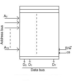
The commercially available memory chips contain a much larger number of cells. As for example, a memory unit of 1MB (mega byte) size, organised as 1M x 8, contains  memory cells. It has got 220 memory location and each memory location contains 8 bits information. The size of address bus is 20 and the size of data bus is 8.
The number of pins of a memory chip depends on the data bus and address bus of the memory module. To reduce the number of pins required for the chip, we use another scheme for address decoding. The cells are organized in the form of a square array. The address bus is divided into two groups, one for column address and other one is for row address. In this case, high- and low-order 10 bits of 20-bit address constitute of row and column address of a given cell, respectively. In order to reduce the number of pin needed for external connections, the row and column addresses are multiplexed on ten pins. During a Read or a Write operation, the row address is applied first. In response to a signal pulse on the Row Address Strobe (RAS) input of the chip, this part of the address is loaded into the row address latch.
All cell of this particular row is selected. Shortly after the row address is latched, the column address is applied to the address pins. It is loaded into the column address latch with the help of Column Address Strobe (CAS) signal, similar to RAS. The information in this latch is decoded and the appropriate Sense/Write circuit is selected.