Basics: In this chapter we will learn the details of testing a IC during and after fabrication. We will also learn that some of the chips which are sold with different speeds such as 2.6 GHz or 2.8 GHz may come from the same wafer. At the end of manufacturing line, each chip will be thoroughly tested. There is no one test which says that the chip is functioning or not functioning. We know that a chip contains millions of transistors. These transistors are not tested one by one, but instead the chip is divided into blocks and each block is tested thoroughly.
For example a processor chip may be divided into few blocks called memory, logic, timer or clock. And in few other chips there is also a part called analog. This logic block or the memory block can also be subdivided into smaller blocks and tested separately. We can use an example to understand the testing and sorting or separating process. Consider a T-shirt manufacturing facility for a particular design. In this facitly, for a particular design, large, medium and small T-shirts may be made. The large will need a lot of cloth, medium, less amount of cloth and the small, the least cloth. Hence the large will be sold at a higher price, the medium at intermediate price and the small at a lowest price.
If thousands of large sized shirts are made, all of them will be checked for quality and the ones with slight damage may be sold under discounted price. Similarly, quality check will be done for the small and the medium sized T-shirts. The shirts which are passing all the tests (i.e. without even the slightest damage) will be sold at high price; the ones with slight damage will be sold at discounted price. If any shirt has lot of damage, it has to be thrown away. For example, if a large size T-shirt is severely damaged, it cannot be sold as a medium size T-shirt (even though the medium size T-shirt is lower priced). A “poor quality large sized T-shirt” cannot be sold as an “acceptable quality medium sized T-shirt”. Next, if we find that, on a particular day, many T-shirts are damaged, then we have to find out the cause of this. Then we can take necessary action to eliminate or at least minimize the damage.
Now let us consider testing in the context of IC manufacturing. A company such as Intel or AMD makes processor chips. They are sold with specifications such as a speed of 3 GHz, 3.2 GHz or 2.8 GHz. A chip may be designed to run at 3.2 GHz. During testing, if it runs as per design, it will be sold as 3.2 GHz. If it does not run well but it is able to run at 3GHz, then the same chip will be sold as a 3 GHz. It is equivalent to selling as slightly damaged T-shirt, but still of acceptable quality, at the discounted price. But remember that one cannot sell a severely damaged T-shirts. Similarly if the 3.2 GHz chip does not work at 3.2 or 3, then the manufacturing company cannot sell it as 2.8 GHz chip. It has to thrown away. The company will have a separate design for a chip running at 2.8 GHz. There good chips will be sold as 2.8 GHz, and slightly poorer quality will be sold as 2.6 GHz and anything which does not satisfy either one speed will be thrown away. Please note that the speed values in GHz are given as examples. The manufacturing companies may not reveal the details.
Now the good chips can be packaged and sold. What is the use of the severely damaged chip? While one cannot use it as a processor, one can analyze it and find the cause of the failure. In the T-shirt analogy, if we find that the damage occur mainly one area, then we can go to the section that area is manufactured, monitor it and find out the source of the problem. Similarly, in the failed chips, we have to find whether any particular block is failing and if it is a design problem or a manufacturing problem (i.e. if some process is not run correctly).
Failure Analysis:
In an IC manufacturing facility, there is a separate section called “failure analysis” (FA) section. There, very sophisticated instruments are used to remove the materials from the failed chips layer by layer and find the exact location of the failure. To do FA, it may take one or two days for a single chip. Thus, many chips cannot be analyzed by this method and just by analyzing few chips, one has to find the major cause of failure.
Scribe line (Parametric testing)
Will all the wafers and chips go through the complete testing? The answer is “no”. Here again an example will help explain the logic behind this answer. Assume that you go to a shop to buy a computer. Let us assume that all the computers are at the table and switched off and that you do not have a firm idea on the model that you want to buy. How would one make a decision about the purchase? First you will switch on the computer, run perhaps an application, or play a movie, or connect to internet and open a website. (You will also look into the specifications and then decide). We can call the initial stages as the superficial testing. If the computer or the monitor or the keyboard looks broken or old, you will not test it at all because you will assume that if it is broken at the outside, it is probably not in good condition. In case you see that all the computers in display look old or broken, even if they are functioning, you will not evaluate the computers there. You will move on to the next shop.
In the same way, for microelectronic chips, a superficial testing will be done at the wafer level. For this purpose, a few transistors and a few resistors are created on the sides of the chips (i.e. between the chips). In the lithography section, we learnt that in a mask there are many chips (Fig 2.18) and that in the gaps between the chips and at the corners, alignment marks are placed In the remaining space between the chips, test structures are used. These are sometimes called kerf or scribe lines and these tests are called parametric tests or process tests. These structures are frequently tested during the process. If these structures fail, then the complete test on the chips will not be done. A ‘batch of wafers’ may contain 25 or 10 or 13 wafers (depending on the size of the wafer. In case of 200 mm wafer, 25 wafers are called a batch. In 300 mm wafers, 10 or 13 wafers are called a batch). If the first two or three wafers are tested parametrically, and if all of them fail, the remaining wafers will not be even tested parametrically or completely. The testing equipment is extremely expensive and there are limited numbers of equipment available in each fab. In order to test each chip and each wafer completely, it takes a significant amount of time. Thus if superficial testing (parametric testing) shows that the structure are likely to be severely damaged, the company will not spend much time and use expensive testing equipment on each and every individual chips because they are likely to be failing chips. The parametric testing is done frequently (e.g. after the transistors are made, then again M1 is made, perhaps after M2 is made and at the end of the manufacturing steps, just before complete test)
Shorts and opens:
The basic tests in the scribeline structures consist of checks for shorts and open. “Shorts” means two metal lines which are supposed to be separated electrically are actually short circuited. “Open” means lines which are supposed to be electrically connected are actually disconnected. The following figures shows the examples of the electrical structures used to check for this. This are commonly called snake or comb and these are made at each metal layer (e.g. poly silicon snakes, M1 snakes or combs, but not via or contact). Only a few such structures are made, which means the ability to estimate the failure is also low. i.e. The process may actually be able to make these simple structures easily but it may not be able to make all the complicated structures in the actual chips fully. But since it is only a superficial test, this estimate is sufficient. A snake structure consists of a single metal line with winds like a snake and this is used for testing for opens (Fig 10.1 (a)). If the line is not continuous because of some problem in the process, then the resistance will be too high or it can be even infinity (if the line is completely broken). There might be tens or hundreds of the test structures and if, 99 out 100 pass, then the quality is considered as ‘acceptable’. If 10 or more out of 100 fail, then the conclusion will be that the process is not good; the logic is, if even for these simple structures 10 out of 100 fail, then we try to make complicated structures (in the actual chip), most likely most of the chips will fail.
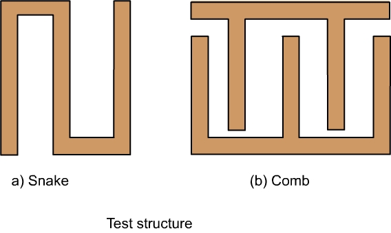
Fig. 10.1. Test structure (a) Snake (b) Comb
To measure the shorts, the structure shown in Fig 10.1 (b) is used. This looks like a comb kept next to another comb, and this whole structure is frequently called comb structure. If the processes are run correctly, then structure will be made properly and there will not be any shorts (current leakage) between these two combs. If there is any short circuit, then there will be leakage currents between these combs.
In the typical fab, these tests will be conducted and the results will be plotted in a particular format, for example as a cumulative density function plot (CDF). These plots are helpful in identifying even a small number of failures. Logarithmic scale is used to identify very small levels such as ppm or ppb levels of defects. When these analyses are performed for test results corresponding to individual modules (such as M1 or M2), they also help in identifying where a problem lies.
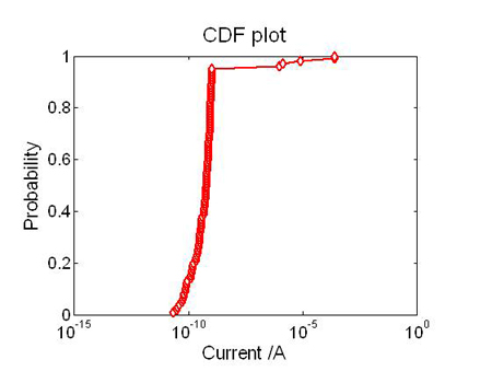
Fig 10.2 Sample CDF plot of leakage current of a structure. If 100 structures are tested, a few may fail (i.e. exhibit high current)
If we know that a chip fails, then it is not sufficiently detailed information. If we know that the chips fails at M1 level for shorts, then it helps in identifying likely sources of the problem and in taking remedial action to correct this. Few other structures are also used in the parametric or the process test. One is called VDP, which is an acronym for Van-der-Pauw. Using this structure, the thickness or the sheet resistance of a deposited material can be determined. Using additional structures, even the width of a line can be estimated. The resistance of a metal line is normally expressed in terms of the resistivity of the material and the length and the cross sectional area of the wire. However in semiconductor processing, we learnt that sheet resistance is used more frequently. At M1, the metal thickness is same for all the lines but the lengths and widths vary. Similarly at M2, they have a different thickness compared to M1 but among all the M2lines, the thickness is the same (but the width and the length vary again). Thus it is clear that in the semiconductor processing the thickness is the same for the given layer, but the width and the length vary.
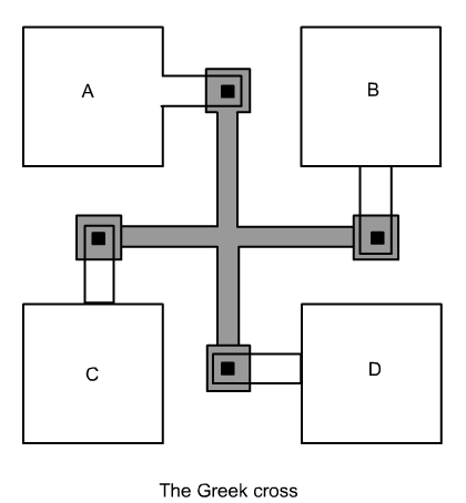
Fig. 10.3. Schematic of a Greek cross (a Van-der-Pauw structure). (REDRAW THE ABOVE FIGURE)
A VDP structure, called Greek cross, is shown in Fig. 10.3. In this, the current is passed between A and B terminals while the potential is measured between terminals C and D. The sheet resistance is calculated as 
Complete test: The complete testing program looks similar to a C program or a script. The testing programs are written in their own language, but most of them are easy to read. They are also normally well commented and will have the information such as the name of the test, the voltage applied, and the device under test (DUT). Apart from the test information, they also have information on the alignment and the x-y movement of the tester. The test pins (wires to pass potential or current to the chip) must be properly aligned. After a chip is tested, the wafer must be moved slightly so that the next chip is placed correctly below the pins. Thus the alignment and x-y movement information are also important. Some of the test may be capacitance-voltage (CV) test for oxide or current-voltage (IV) test. These types of tests are very time consuming and are not done frequently. Most of the tests done on modern chips are digital tests. Some of them are usually referred to by acronyms such as TDDB (temperature dependence dielectric break down), NBTI (negative bias temperature instability) and IDDQ (quiescent supply current) and so on.
Binning (Sort test) : The tested chips (also called dies) are sorted or separated based on the failure modes. This process is called binning or sorting. Remember that a die (i.e. chip) will have blocks such as memory, scan, clock etc. In the production stage, the block which tends to fail more will always be tested first. If it fails, there is no use in testing the chip further. Hence, once a chip fails, it will not be tested further. Based on the block where the failure occurs, and the type of failure, it will be marked. One can imagine that it is thrown into a waste bin or waste bucket; different buckets would be available and each bucket will correspond to a block and a failure mode. There may be one bucket for chips failing in memory. There may be a second bucket for chips failing in the scan region and a third bucket for chips having opens in the analog region. There may be a fourth bucket for a chip failing in the clock region. Even within the buckets, there may be different compartments. Within the scan region, if it fails for too much current, it may go to one compartment, and if it fails for too little current, it may go to another compartment. If a chip passes all the tests, then it is thrown in a ‘good chip’ bucket (i.e. bin).
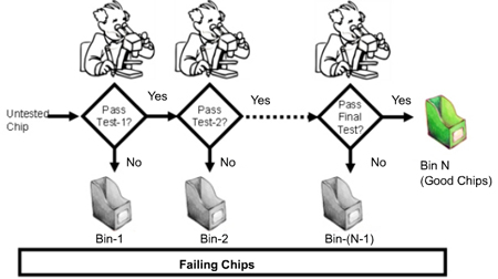
Fig. 10.4 Bin test (or sort test). A simplified illustration
However in practice, none of the chips are physically thrown in buckets. Instead, a computer program will keep track of the mode of failure of each. This process is called binning, because one can imagine that the chips are thrown in different buckets or bins. It we say, it fails in scan region, then we know overall it has gone into the scan bucket. If we also know the compartment within the bucket it has gone into, then we have more detailed data. The buckets are called hard bin and the bucket with compartment information is called soft bin. Hard bin means we know the overall reason about the failure. Soft bin means we also know the compartment in which it has failed or compartment in which it has been placed (i.e. we know the detailed information on the failure).
The binning of failing chips helps to determine the block which fails frequently. Based on the data, the engineer will try to determine the cause of the issue and make the improvements necessary. The actual troubleshooting requires in depth analysis and a lot of experience. Typically, a fab will have a team of experts to perform the ‘yield analysis’ and suggest improvements.
Typical test sequences: Normally the very first tests are the continuity tests to test the short and the open, which will catch the problem if there is a severe shortage or severe open issue. The next test is called built-in-self-test or BIST. Third is typically the sequence of tests which looks into the logic area (also called functional area) and these tests are usually called scan. Most of the chips now have built in memory or embedded memory. The testing for memory is different from the testing for logic in one sense. That is the memory chip can be repaired if there is a failure and the repair will improve the yield dramatically. The memory contains lot of identical circuits called bits. If many bits fail in a memory part, the location of all failing bits can be marked as a pattern. This is called failed bit map (FBM). FBM can help identify the problem in a process, without actually doing failure analysis.
|