We begin with the following observation. The price of most of the things increases every year. Whether it is petrol, or food, or land, or gold, the price usually increases with time. However, a remarkable exception to this trend is the price of electronic goods. The price of a computer or cell phone decreases every year. In addition, the power and functionality of these items becomes more. In fact, some of the ‘old models’ are no longer available and are superseded by new, more powerful and less expensive models. Why do electronic goods show a different trend compared to all other goods?
At the heart of the electronic goods is microelectronic chip or integrated chip (IC). Every year, there is significant advancement in the technology of making these chips. Because of the advancements, the power of the chip increases while the production cost decreases. That is the reason for the decrease in cost of the electronic goods over time.
In this course, we will learn the process steps used in making the IC. First, we will see a brief history of ICs. In 1947, William Shockley, John Bardeen and Walter Brattain invented a device called transistor. It is somewhat like a switch, in the sense it can be turned ‘on’ or ‘off’. Before the invention of transistors, electrical circuits consisting of resistances, capacitances and triodes (using vacuum tubes) were used in making radios and televisions. They were bulky, expensive and used a lot of electricity. In the beginning, the transistors were made separately and were connected using wires. In this method, it was not possible to make many circuits. Then in 1957, Jack Kilby created five transistors simultaneously and formed a circuit. Since all the transistors of the circuits are created simultaneously, this is called ‘integrated chip’. The difference between creating the transistors separately and creating them together can be illustrated with the following analogy. If we use a type writer to write a letter, then each letter has to be typed one by one. If we want to make 10 such letters, then it takes a long time to do that in the typewriter. On the other hand, in a printing press, all the letters of a page are arranged. The initial preparation takes some time. But once the letter is ready, making 10 or more copies is fast. Similarly, making transistors one by one is relatively simple, but time consuming task. Making all the transistors together is a bit more complex process, but when many such replicas are produced, it saves a lot of time. After Jack Kilby, Rober Noyce improved the manufacturing process. Now, many millions of transistors are routinely created in a single integrated chip.
The transistors are made in materials which are relatively poor conductors of electricity and are classified as semiconductors. Elements such as silicon (Si) or germanium (Ge) are semiconductors. Compounds such as gallium arsenide (GaAs) are also semiconductors. The first transistor was made using germanium. However, at present, most of the chips are made using silicon. Some of the reasons for this is (a) the easy availability of silicon (sand is impure form of silicon dioxide) and (b) the formation of a good quality silicon-di-oxide (SiO2) on top of silicon. The SiO2 layer forms automatically when Si is exposed to air or water. It offers good protection from chemical attack and also serves as an excellent insulator. In this course, we focus our attention on the processes relevant for creating silicon based microelectronic chips.
In the making of an IC, a variety of processes are involved. The silicon is in the form of a thin wafer. A Si wafer may be of 200 mm diameter and 0.45 mm thick, or 300 mm diameter and 1 mm thick. Currently most manufacturers use 300 mm wafers, while a few still employ 200 mm wafer. Thus, a typical wafer will be of the size of a plate, but with less thickness. The material is fragile and hence should be handled carefully. Although the wafer thickness is at least 0.45 mm, the transistors are made within the first micron or less. Thus, only 0.1% of the entire thickness of the wafer is used. The remaining is used mainly for mechanical strength. If the wafer is made with less thickness, it is likely to break very easily during handling. The silicon atoms are arranged in a periodic manner and this is called single crystalline silicon. If the crystal structure is periodic for a short distance (e.g. microns) but if there are breaks in longer distances, it is called poly crystalline. If the distance between the atoms varies even in short distances, it is amorphous. For IC industry, single crystalline silicon is used as the base.
The transistors are made on the wafer by adding certain materials (such as boron or phosphorous). We will learn the details in the later chapters. Once the transistors are made, they have to be connected properly using conducting wires. The wires should also be insulated. Otherwise, there will be short circuits and the chip will not function. Previously aluminum was used as the conducting material, but now copper is used as the conductor. These are called “interconnects”. The insulator is used previously is silicon di oxide, but now new materials called “low-k” materials are being used in the advanced chips. These are usually organic materials, which have a low dielectric constant.
In the manufacturing line, the transistors are made first and then the interconnects are made. The processes involved in making the transistors are called Front End Of Line (FEOL) and the process of making the interconnects are called Back End Of Line (BEOL). While transistors are made in one level (one layer) of the wafer, the interconnects can not be made in one level, since the connections are very complex. The interconnects are made in 4 or more levels and some of the advanced chips use up to 9 levels of interconnects. The following figure shows a schematic with four devices connected in two levels. A device may be a transistor or a diode. Although a transistor will have three connections and a diode will have two connections, the following figure shows only one connection per device for the sake of simplicity.
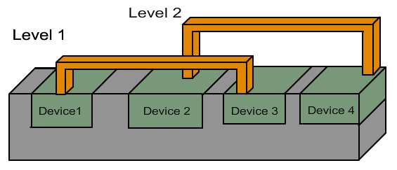
Fig 1.1 Schematic showing one level of transistor and 2 levels of interconnects
In the interconnects, the vertical wires touching the transistors are called ‘contacts’. Usually they are made of tungsten (W). All the other vertical wires (i.e. connecting first level and second level, or connecting “N”th level to “N+1”st level) are called ‘vias’. The horizontal wires are called ‘metal lines’ or sometimes just ‘metal’.
Fig 1.2 Schematic showing via and metal lines
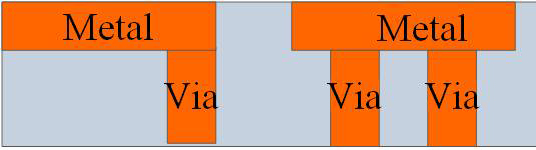
In the industry jargon, M1 refers to “metal lines at level 1”, M2 refers to “metal lines at level 2” and so on. Similarly, “via12” refers to via layer connecting M1 and M2, ‘via23’ refers to via layer connecting metal 2 to metal 3 and so on. The layer connecting the transistor and M1 are referred to as “contacts” as we noted earlier. When the interconnect metal is aluminum, all the ‘metal lines’ are made of aluminum, while all the contacts and vias are made of tungsten. When the interconnect metal is copper, all the metal lines and vias are made of copper, but the contacts are still made with tungsten.
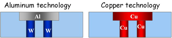
Fig 1.3 Schematic showing “via” material and “metal line” material for Al and Cu technology
Since the transistors are very small, the length units usually used in the industry are micron (1μ=10-6 m), nanometer (1 nm = 10-9 m) or angstrom (1 Å = 10-10 m). Many millions are transistors are present in an IC and a wafer may have a few hundred chips. The thickness of the interconnect wires may be of the order of 100 nm or so and length may be several microns. It is not possible to add materials of exact size only in the places where want. Thus, a typical process sequence will involve adding a material to the wafer and removing excess material from unwanted places.
In order to make a transistor, the silicon has to be modified, by adding boron or phosphorous in specific locations. Thus, the location where these materials must be added (or removed) must also be specified. Thus, we need processes to add materials, to remove materials, to modify the silicon and to specify the locations (pattern definition). The process used to define the locations is called photo lithography and is a key process in chip manufacturing. The most common processes used for material addition are physical vapor deposition (PVD), chemical vapor deposition (CVD), electrochemical deposition (ECD) and spin-on coating. The typical removal processes are wet etching, dry etching, and chemical mechanical planarization. Diffusion, ion implantation and oxidation are the material modification processes. All these processes must be implemented carefully so that the chips are made correctly. Once the ICs are made, they are tested to ensure that they function correctly and if any of them fail during the test, they are analyzed to understand the cause of failure. This helps to improve the processes and increase the success rate.
In this course, we will first learn the various processes used in the semiconductor industry. The overall steps can be understood with the help of an analogy. Let us assume that we want to build a college. First we have to decide whether it will be an Engineering college or a medical college or a science college. We also have to know approximately how many students would be enrolled in it and so on. Based on that, one can decide the number of class rooms, the number of labs, office rooms, hostel facilities and so on. This can be viewed as the first stage. At this stage, the exact location of the rooms and labs will not be clear, but only the overall information will be available.
In the second stage, with the help of an architect, the blue print or the layout of the college will be decided. Now, the exact location of each room will be known ‘on paper’. This can be considered as second stage. In the third stage, the college and other facilities will be built, with the help of civil engineers. At the fourth and final stage, we will inspect the college to ensure that everything is ready and inaugurate it.
A chip manufacturing process can also be viewed similarly. In the first stage, the electronics engineers will design, for example, a cell phone chip. The number of transistors and diodes and resistances in the circuit will be known, but the exact location will not be decided. In the second stage, the electrical circuit will be converted into a physical layout. Now, the exact location of each transistor and other devices will be known. However, it is only ‘on paper’ (in this case, ‘soft copy’). In the third stage, there is a difference between the college example and chip manufacturing. In IC manufacturing, millions of chips must be made. So, at the end of second stage, a set of ‘masks’ will be made and from the masks, using various processes, millions of chips will be made. This process can also be thought of as printing many copies of photos from a negative. The course focuses mainly on the details of the third stage. At the end, the chips will be tested and the passing chips will be sold. This is somewhat similar to the fourth stage in the example.
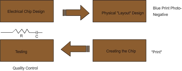
Fig 1.4. Major steps in integrated chip manufacturing
Most of the processes are common to making the transistor (FEOL) and making the interconnects (BEOL). The common processes such as lithography, deposition and removal will be presented first. Then the basics of semiconductor, transistor’s structure and operation and transistor formation will be discussed. A few processes specific to FEOL, such as diffusion, oxidation and ion implantation will be presented afterwards.
This is in contrast to what one would see in traditional books on this topic. Usually, the process of making a single crystal silicon wafer would be presented first. Next the process sequence for fabricating a transistor (FEOL processes) would be presented along with the details of the processes. Finally, a brief view of the processes used in creating the interconnects (BEOL processes) would be given. We have made a deliberate choice of presenting the BEOL processes first. This is because the concepts of electrical conductors and insulators are very simple and those with Chemical Engineering or similar background can easily follow the requirements of the processes involved in BEOL part. Then the structure and operation of the transistor is introduced. By that time, the audience would have been familiar with many of the thin film processes which are common for BEOL and FEOL. Finally, the processes unique to FEOL are introduced. Based on almost 10 years of teaching undergraduate and postgraduate students with Chemical Engineering background, I find this to be more effective than the traditional sequence of presentation. A process engineer in an IC fabrication plant never sees the process of making silicon wafer since it is directly purchased from suppliers. The silicon wafer making industry is considered as an allied industry and hence those details are also not presented here.
We will also learn the basics of testing and analyzing the test results using yield modeling. Finally, a brief overview of the tools and techniques used in microelectronic industry will be presented at the end. |