Spin on coating:
This method is used for depositing organic materials. The equipment is similar to the tool used in lithography for coating photo resist on to the wafer. First, the material to be deposited is dissolved in a solvent such as acetone or ethanol. Next, the wafer is kept on a platform and is rotated at about 500 rpm. While the wafer is spinning, the solution is poured on the wafer. Due to the rotation, the solution will spread on the wafer. Then the wafer is rotated at higher speed (about 5000 rpm). This controls the thickness of the solution. If the wafer is also heated, the solvent will evaporate, leaving the material on top of the wafer in the form of a film.
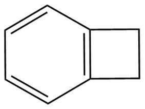
Traditionally silicon dioxide is used as the insulator between copper wires. Recently some materials called low-k materials, which have low dielectric constant, are used as insulators. Some examples of low-k materials are poly-tetrafluroethylene (PTFE, also called Teflon), benzo cyclobutene and polyimide (structure given below) This enables the chip to run faster and reduce the electrical current loss. Spin-on method is used to deposit the low-k materials.
 .jpg)
(a) (b)
Fig 3.21 Structure of (a) benzocyclobutene and (b) imide
In the next section, we will see the techniques used to remove excess materials, under the topic “removal methods”.
|