Atomic Layer Deposition: ALD can be thought of as a CVD technique with precise flow control. Consider a reaction between water vapor and trimethyl aluminum (TMA) to produce alumina (Al2O3) layer. The overall reaction is

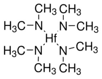
If both reactants are supplied to the chamber containing wafer, alumina layer will form on the wafer, but the thickness will not be easy to control. However, in ALD, first only water vapor is sent to the chamber. A monolayer of water will chemisorb onto the wafer. Then the chamber is evacuated and all the water vapor present, except the adsorbed molecules, will be removed. Next, a pulse of TMA is introduced in the chamber. Now, the TMA will react with limited water molecules present on the wafer and produce exactly one layer of alumina. The chamber is evacuated again and the water vapor and TMA are sent in sequence to grow the exact number of alumina layers required. At present, ALD is used for growing gate oxides in the advanced chips. Instead of SiO2, other materials such as HfO2 (hafnium oxide) are used as gate oxide in these chips and ALD offers the control necessary to deposit thin layers. The reaction between tetrakis dimethyl amido hafnium (structure given below) and water or ozone results in hafnium oxide.

Similarly, tetrakis dimethyl amido zirconium and water can be used as two reactants to obtain zirconia (zirconium oxide) in ALD.
|