In order to make a transistor, the silicon has to be modified, by adding boron or phosphorous in specific locations. Thus, the location where these materials must be added (or removed) must also be specified. Thus, we need processes to add materials, to remove materials, to modify the silicon and to specify the locations (pattern definition). The process used to define the locations is called photo lithography and is a key process in chip manufacturing. The most common processes used for material addition are physical vapor deposition (PVD), chemical vapor deposition (CVD), electrochemical deposition (ECD) and spin-on coating. The typical removal processes are wet etching, dry etching, and chemical mechanical planarization. Diffusion, ion implantation and oxidation are the material modification processes. All these processes must be implemented carefully so that the chips are made correctly. Once the ICs are made, they are tested to ensure that they function correctly and if any of them fail during the test, they are analyzed to understand the cause of failure. This helps to improve the processes and increase the success rate.
In this course, we will first learn the various processes used in the semiconductor industry. The overall steps can be understood with the help of an analogy. Let us assume that we want to build a college. First we have to decide whether it will be an Engineering college or a medical college or a science college. We also have to know approximately how many students would be enrolled in it and so on. Based on that, one can decide the number of class rooms, the number of labs, office rooms, hostel facilities and so on. This can be viewed as the first stage. At this stage, the exact location of the rooms and labs will not be clear, but only the overall information will be available.
In the second stage, with the help of an architect, the blue print or the layout of the college will be decided. Now, the exact location of each room will be known ‘on paper’. This can be considered as second stage. In the third stage, the college and other facilities will be built, with the help of civil engineers. At the fourth and final stage, we will inspect the college to ensure that everything is ready and inaugurate it.
A chip manufacturing process can also be viewed similarly. In the first stage, the electronics engineers will design, for example, a cell phone chip. The number of transistors and diodes and resistances in the circuit will be known, but the exact location will not be decided. In the second stage, the electrical circuit will be converted into a physical layout. Now, the exact location of each transistor and other devices will be known. However, it is only ‘on paper’ (in this case, ‘soft copy’). In the third stage, there is a difference between the college example and chip manufacturing. In IC manufacturing, millions of chips must be made. So, at the end of second stage, a set of ‘masks’ will be made and from the masks, using various processes, millions of chips will be made. This process can also be thought of as printing many copies of photos from a negative. The course focuses mainly on the details of the third stage. At the end, the chips will be tested and the passing chips will be sold. This is somewhat similar to the fourth stage in the example.
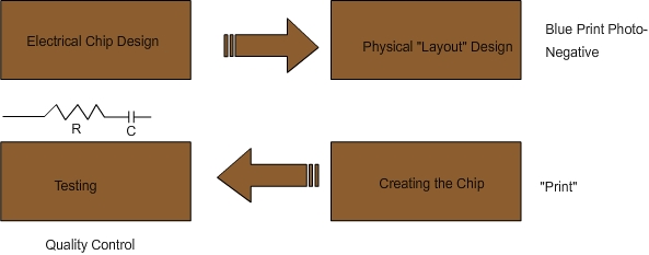
Fig 1.4. Major steps in integrated chip manufacturing
Most of the processes are common to making the transistor (FEOL) and making the interconnects (BEOL). The common processes such as lithography, deposition and removal will be presented first. Then the basics of semiconductor, transistor’s structure and operation and transistor formation will be discussed. A few processes specific to FEOL, such as diffusion, oxidation and ion implantation will be presented afterwards. We will also learn the basics of testing and analyzing the test results using yield modeling. Finally, a brief overview of the tools and techniques used in microelectronic industry will be presented at the end. |