In the manufacturing line, the transistors are made first and then the interconnects are made. The processes involved in making the transistors are called Front End Of Line (FEOL) and the process of making the interconnects are called Back End Of Line (BEOL). While transistors are made in one level (one layer) of the wafer, the interconnects can not be made in one level, since the connections are very complex. The interconnects are made in 4 or more levels and some of the advanced chips use up to 9 levels of interconnects. The following figure shows a schematic with four devices connected in two levels. A device may be a transistor or a diode. Although a transistor will have three connections and a diode will have two connections, the following figure shows only one connection per device for the sake of simplicity.
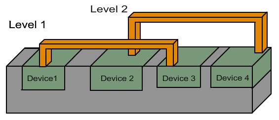
Fig 1.1 Schematic showing one level of transistor and 2 levels of interconnects
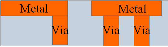
In the interconnects, the vertical wires touching the transistors are called ‘contacts’. Usually they are made of tungsten (W). All the other vertical wires (i.e. connecting first level and second level, or connecting “N”th level to “N+1”st level) are called ‘vias’. The horizontal wires are called ‘metal lines’ or sometimes just ‘metal’.
Fig 1.2 Schematic showing via and metal lines
In the industry jargon, M1 refers to “metal lines at level 1”, M2 refers to “metal lines at level 2” and so on. Similarly, “via12” refers to via layer connecting M1 and M2, ‘via23’ refers to via layer connecting metal 2 to metal 3 and so on. The layer connecting the transistor and M1 are referred to as “contacts” as we noted earlier. When the interconnect metal is aluminum, all the ‘metal lines’ are made of aluminum, while all the contacts and vias are made of tungsten. When the interconnect metal is copper, all the metal lines and vias are made of copper, but the contacts are still made with tungsten.
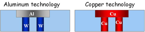
Fig 1.3 Schematic showing “via” material and “metal line” material for Al and Cu technology
Since the transistors are very small, the length units usually used in the industry are micron (1 = 10-6 m), nanometer (1 m = 10-9 m) or angstrom (1 Å = 10-10 m). Many millions are transistors are present in an IC and a wafer may have a few hundred chips. The thickness of the interconnect wires may be of the order of 100 nm or so and length may be several microns. It is not possible to add materials of exact size only in the places where want. Thus, a typical process sequence will involve adding a material to the wafer and removing excess material from unwanted places. = 10-6 m), nanometer (1 m = 10-9 m) or angstrom (1 Å = 10-10 m). Many millions are transistors are present in an IC and a wafer may have a few hundred chips. The thickness of the interconnect wires may be of the order of 100 nm or so and length may be several microns. It is not possible to add materials of exact size only in the places where want. Thus, a typical process sequence will involve adding a material to the wafer and removing excess material from unwanted places. |