We can do away with the center tap and therefore use a single a.c. supply to the circuit by the use of a slightly more complicated circuit invloving four dioded as shown above.
![\includegraphics[width=3.5in]{lec8figs/17.eps}](img611.png)
The diode D2 and D3 conduct in the positive half cycle while D1 and D4 in the negative half cycle. when the load is purely resistive. The output is the same as center tapped transformer based full wave rectifier.
We started with the objective of getting a ripple free waveform at the output. We notice that in the circuits that we have discussed so far, this aim is not achieved and the primary reason for that is the change in output voltage as the input voltage changes. We overcome this shortcoming by the use of Energy Storage Elements whose function is to absorb energy at higher voltages and release it at lower voltages, thereby reducing the ripple factor..
Examples of such elements are inductors and capacitors. The circuit below shows the configuration of a full wave rectifier with a capacitor.
Without any load, the capacitor once charged remains charges and therefore the ripple factor become zero.
Now,if a load ![]() is connected, some amount of discharging of the capacitor takes place in each half cycle. The magnitude of the ripple factor therefore depends on the
is connected, some amount of discharging of the capacitor takes place in each half cycle. The magnitude of the ripple factor therefore depends on the ![]() and
and ![]() .
.
![\includegraphics[width=3.5in]{lec8figs/22.eps}](img616.png)
Neglecting the voltage discharge that takes place after the completion during the next cycle, i.e. from the point ![]() onwards, we get, at
onwards, we get, at ![]() ,
,
![]() , where
, where ![]() . Therefore,
. Therefore,
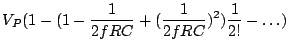 |
Neglecting the square and higher terms for
![]() , we get,
, we get,

![\includegraphics[width=3.5in]{lec8figs/24.eps}](img628.png)
From the figure above, the average value of the voltage can be approximated to be
![]() . Therefore,
. Therefore,
 |
|||
 |
|||
 |
When ![]() ,
,
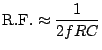
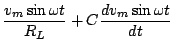
Next, we will consider the diode current calculations.
![\includegraphics[width=3.5in]{lec8figs/32.eps}](img636.png)
![\includegraphics[width=3.5in]{lec8figs/33.eps}](img637.png)
In the period P, the diode current, ![]() is given bym
is given bym
 |
|||
 |
|||
 |
|||
![\includegraphics[width=3.5in]{lec8figs/34.eps}](img648.png)
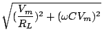
Note that the peak diode current, ![]() , increases with reduction in
, increases with reduction in ![]() or increase in
or increase in ![]() or
or ![]() .
.
We see that as ![]() reduces, R.F. increases.But it cannot become zero for finite resistances. A way to achieve a better (smaller) ripple factor is through the use of a Zener Diode
reduces, R.F. increases.But it cannot become zero for finite resistances. A way to achieve a better (smaller) ripple factor is through the use of a Zener Diode
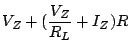
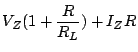
The zener diode when connected in parallel with the load makes the load voltage approximately equal to the zener voltage (
![]() )as long as it is reverse biased. This happens if and only if the voltage across the capacitor is greater than the zener voltage.
)as long as it is reverse biased. This happens if and only if the voltage across the capacitor is greater than the zener voltage.
For this condition to be met, we must have
 |
|||
 |
|||
 |
When ![]() ,
, ![]() and when
and when ![]() ,
,
![]() .
.
![\includegraphics[width=3.5in]{lec8figs/28.eps}](img663.png)
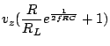
For the figure above, slope =
![]() . When discharge rate is higher so that at some point,
. When discharge rate is higher so that at some point, ![]() becomes less than
becomes less than ![]() , then,
, then, ![]() goes below
goes below ![]() as shown below
as shown below
When the capacitor voltage is less than the input voltage, the diodes are input dioded are in cutoff and the capacitor sees the following discharge circuit for the case when
![]() .i.e.
.i.e.
![]() . In this case,
. In this case,
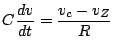
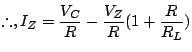
In the above case,
 |
|||
 |
|
|||
 |
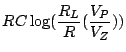
Example: If ![]() volts,
volts,
![]() ,
, ![]() and
and ![]() mF, we must have
mF, we must have
![]() V. Conversely, for a given
V. Conversely, for a given ![]() , one can find a range of
, one can find a range of ![]() for no ripples.
for no ripples.
![\includegraphics[width=3.5in]{lec8figs/30.eps}](img689.png)
![\includegraphics[width=3.5in]{lec8figs/16.eps}](img610.png)
![\includegraphics[width=3.5in]{lec8figs/18.eps}](img612.png)
![\includegraphics[width=3.5in]{lec8figs/19.eps}](img613.png)
![\includegraphics[width=3.5in]{lec8figs/20.eps}](img614.png)
![\includegraphics[width=3.5in]{lec8figs/23.eps}](img617.png)
![\includegraphics[width=3.5in]{lec8figs/26.eps}](img652.png)
![\includegraphics[width=3.5in]{lec8figs/27.eps}](img654.png)
![\includegraphics[width=3.5in]{lec8figs/29.eps}](img668.png)