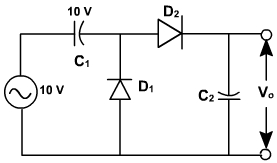
Voltage Doubler :
A voltage doubler circuit is shown in fig. 5. The circuit produces a dc voltage, which is double the peak input voltage.
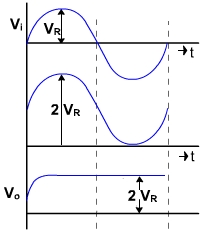
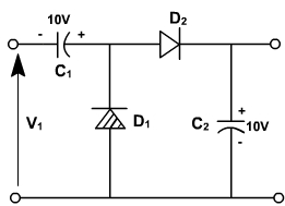
Fig. 5 Fig. 6 At the peak of the negative half cycle D1 is forward based, and D2 is reverse based. This charges C1 to the peak voltage Vp with the polarity shown. At the peak of the positive half cycle D1 is reverse biased and D2 is forward biased. Because the source and C1 are in series, C2 will change toward 2Vp. e.g. Capacitor voltage increases continuously and finally becomes 20V. The voltage waveform is shown in fig. 6.
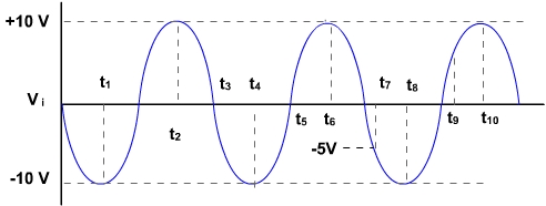
To understand the circuit operation, let the input voltage varies from -10 V to +10 V. The different stages of circuit from 0 to t10 are shown in fig. 7(a).
Fig. 7(a)
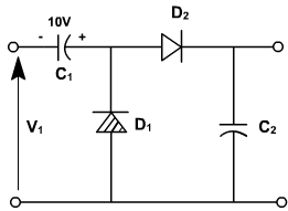
During 0 to t1, the input voltage is negative, D1 is forward biased the capacitor is charged to 10 V with the polarity as shown in fig. 7b.
Fig. 7(b)
During t1 to t2, D2 becomes forward biased and conducts and at t2, when Vi is 10V total voltage change is 20V. If C1 = C2 = C, both the capacitor voltages charge to +10 V i.e. C1 voltage becomes 0 and C2 charges to +10V.
Fig. 7(c)
From t2 to t3 there is no conduction as both D1 and D2 are reverse biased.
During t3 to t4 D1 is forward biased and conducts. C1 again charges to +10V
Fig. 7(d)
During t4 to t5 both D1 and D2 are reverse biased and do not conduct.
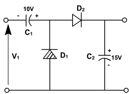
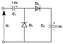
During t5 to t6 D2 is forward biased and conducts. The capacitor C2 voltage becomes +15 V and C1 voltage becomes +5 V.
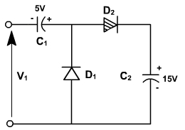
Fig. 7(e)
Again during t6 to t7 there is no conduction and during t7 to t8, D1 conducts. The capacitor C1 recharges to 10 V.
Fig. 7(f)
During t8 to t9 both D1 and D2 are reverse biased and there is no conduction.
During t9 to t10 D2 conducts and capacitor C2 voltage becomes + 17.5 V and C1 voltage becomes 7.5V. This process continues till the capacitor C1 voltage becomes +20V.
Fig. 7(g)