Example - 1:
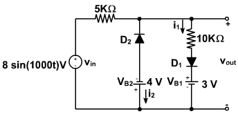
Find the output voltage v out of the clipper circuit of fig. 7(a) assuming that the diodes are
- ideal.
- Von = 0.7 V. For both cases, assume RF is zero.
 |
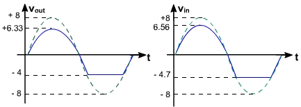 |
|---|---|
| Fig. 7(a) | Fig. 7(b) |
Solution:
(a). When vinis positive and vin < 3, then vout = vin
and when vin is positive and vin > 3, then
At vin = 8 V(peak), vout = 6.33 V.
When vinis negative and vin > - 4, then vout = vin
When vin is negative and vin < -4, then vout = -4V
The resulting output wave shape is shown in fig. 7(b).
(b). When VON = 0.7 V, vin is positive and vin < 3.7 V, then vout = vin
When vin > 3.7 V, then
When vin = 8V, vout = 6.56 V.
When vin is negative and vin > -4.7 V, then vout = vin
When vin < - 4.7 V, then vout = - 4.7 V
The resulting output wave form is shown in fig. 7(b).
Clamper Circuits:
Clamping is a process of introducing a dc level into a signal. For example, if the input voltage swings from -10 V and +10 V, a positive dc clamper, which introduces +10 V in the input will produce the output that swings ideally from 0 V to +20 V. The complete waveform is lifted up by +10 V.
Negative Diode clamper:
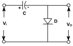
A negative diode clamper is shown in fig. 8, which introduces a negative dc voltage equal to peak value of input in the input signal.
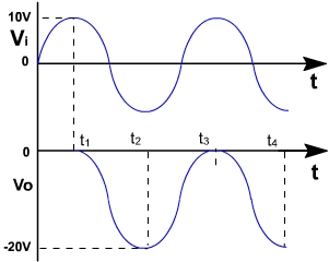
Fig. 8 Fig. 9 Let the input signal swings form +10 V to -10 V. During first positive half cycle as V i rises from 0 to 10 V, the diode conducts. Assuming an ideal diode, its voltage, which is also the output must be zero during the time from 0 to t1. The capacitor charges during this period to 10 V, with the polarity shown.
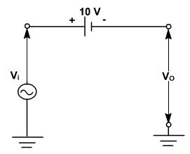
At that Vi starts to drop which means the anode of D is negative relative to cathode, ( VD = vi - vc ) thus reverse biasing the diode and preventing the capacitor from discharging. Fig. 9. Since the capacitor is holding its charge it behaves as a DC voltage source while the diode appears as an open circuit, therefore the equivalent circuit becomes an input supply in series with -10 V dc voltage as shown in fig. 10, and the resultant output voltage is the sum of instantaneous input voltage and dc voltage (-10 V).
Fig. 10


