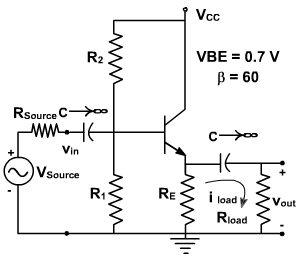
Example-1
Design a single stage npn emitter follower amplifier as shown in fig. 2 with β =60, VBE =0.7V, Rsource =1 KΩ, and VCC= 12V. Determine the circuit element values for the stage to achieve Ai = 10 with a 100 Ω load.
Fig. 2
Solution:
We must select R1, R2 and RE, but we only have two equations. These two equations are specified by the current gain and the placement of the Q-point.
As discussed earlier, the best choice for a CE amplifier is to make RC =R load. We could derive a similar result for RE and Rload in the CC amplifier. We shall therefore begin by constraining REto be equal to Rload. This yields a third equation,
RE = Rload= 100 W
Now finding the load line slopes,
Rac = RE || Rload =50 W
Rdc = RE = 100 V
Since the amplitude of the input is not specified, we choose the quiescent current to place the Q-point in the center of the ac load line for maximum swing.
We now find the value of r'e
Since re is insignificant compared to RE || Rload, it can be ignored. This is usually the case for emitter follower circuits.
Using the equation for current gain we find
Everything in this equation is known except RB. We solve for RB with the result
RB = 1500 W
VBB is found from the base loop.
Continuing with the design as discussed earlier, we find
R1 = 13.8 K Ω
R2 = 1.68 K Ω
The voltage gain of the CC amplifier is approximately unity.
The input resistance is given by
Rin = RB || [ β ( R E || Rload ) ] = 1 kΩ
The output resistance is given by
The maximum peak to peak symmetrical output swing is given by
Vout(p-p) 1.8 | ICQ| (RE || Rload ) = 7.2 V
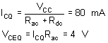
The power dissipated in the load, Pload, and the maximum power required of the transistor, Ptransistor, are