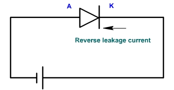
The symbol of diode is shown in fig. 4. The terminal connected to p-layer is called anode (A) and the terminal connected to n-layer is called cathode (K) |
Fig.4 |
Reverse Bias:
If positive terminal of dc source is connected to cathode and negative terminal is connected to anode, the diode is called reverse biased as shown in fig. 5.
Fig.5
When the diode is reverse biased then the depletion region width increases, majority carriers move away from the junction and there is no flow of current due to majority carriers but there are thermally produced electron hole pair also. If these electrons and holes are generated in the vicinity of junction then there is a flow of current. The negative voltage applied to the diode will tend to attract the holes thus generated and repel the electrons. At the same time, the positive voltage will attract the electrons towards the battery and repel the holes. This will cause current to flow in the circuit. This current is usually very small (interms of micro amp to nano amp). Since this current is due to minority carriers and these number of minority carriers are fixed at a given temperature therefore, the current is almost constant known as reverse saturation current ICO.
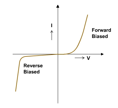
In actual diode, the current is not almost constant but increases slightly with voltage. This is due to surface leakage current. The surface of diode follows ohmic law (V=IR). The resistance under reverse bias condition is very high 100k to mega ohms. When the reverse voltage is increased, then at certain voltage, then breakdown to diode takes place and it conducts heavily. This is due to avalanche or zener breakdown. The characteristic of the diode is shown in fig. 6.
Fig.6
Forward bias:
When the diode is forward bias, then majority carriers are pushed towards junction, when they collide and recombination takes place. Number of majority carriers are fixed in semiconductor. Therefore as each electron is eliminated at the junction, a new electron must be introduced, this comes from battery. At the same time, one hole must be created in p-layer. This is formed by extracting one electron from p-layer. Therefore, there is a flow of carriers and thus flow of current.


