The maximum power dissipated in this type of series regulator is the power dissipated in the internal pass transistor, which is approximately (VS max - Vout) IL max. Hence, as the load current increases, the power dissipated in the internal pass transistor increases. If ILoad exceeds 0.75 A, the IC package should be secured to a heat sink. When this is done, ILoad can increase to about 1.5 A.
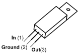
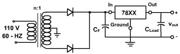
We now focus our attention on the 78XX series of regulators. The last two digits of the IC part number denote the output voltage of the device. Thus, for example, a 7808 IC package produces an 8V regulated output. These packages, although internally complex, are inexpensive and easy to use.There are a number of different voltages that can be obtained from the 78XX series 1C; they are 5, 6, 8, 8.5, 10, 12, 15, 18, and 24 V. In order to design a regulator around one of these ICs, we need only select a transformer, diodes, and filter. The physical configuration is shown in fig. 3(a). The ground lead and the metal tab are connected together. This permits direct attachment to a heat sink for cooling purposes. A typical circuit application is shown in fig. 3(c).
(a)
(b)
(c)
Fig. 3
The specification sheet for this IC indicates that there must be a common ground between the input and output, and the minimum voltage at the IC input must be above the regulated output. In order to assure this last condition, it is necessary to filter the output from the rectifier. The CF in fig. 3(b) performs this filtering when combined with the input resistance to the IC. We use an n:1 step down transformer, with the secondary winding center-tapped, to drive a full-wave rectifier.
The minimum and maximum input voltages for the 78XX family of regulators are shown in Table-1.
Table - 1
We use Table -1 to select the turns ratio, n, for a 78XX regulator. As a design guide, we will take the average of Vmax and Vmin of the particular IC regulator to calculate n. For example, using a 7805 regulator, we obtain
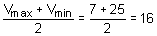
The center tap provides division by 2 so the peak voltage out of the rectifier is 115 √2 / 2n = 16. Therefore, n = 5. This is a conservative method of selecting the transformer ratio.
The filter capacitor, CF, is chosen to maintain the voltage input range to the regulator as specified in Table 8.1.
The output capacitor, CLoad, aids in isolating the effect of the transients that may appear on the regulated supply line. CLoad should be a high quality tantalum capacitor with a capacitance of 1.0 µF. It should be connected close to the 78XX regulator using short leads in order to improve the stability performance.
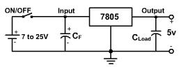
This family of regulators can also be used for battery powered systems. Fig. 3(c) shows a battery powered application. The value of CF is chosen in the same manner as for the standard filter.
The 79XX series regulator is identical to the 78XX series except that it provides negative regulated voltages instead of positive.
Example-1
Design an IC circuit regulator to generate a 12 V output into a load whose current varies from 100 mA to 500 mA. The input is 115 V rms at 60 HZ.
Solution:
We use the circuit of fig. 3(b) with a 7812 regulator. The center-tapped transformer and full-wave rectifier must produce a minimum voltage of at least 14.5 V and a maximum voltage of no more than 30V. This information is obtained from Table 8.1. The input peak voltage is 115 √2 or 163 V. The center-tapped secondary divides this by 2 to yield 81.5V. Let us choose the mid-point between 14.5 and 30, or 22.25 V to select the transformer ratio. This yields a transformer ratio of 81.5 / 22.25 or 3.68.
Since Vs min= 14.5 V (from Table 8.1) and Vs max= 22.3 V, we have
We have used the fact that
ΔV = 22.3 14.5 = 7.8 V
and
Rload (worst case) = 29Ω
The value of C load is determined by the types of variations that occur in the load. A typical selection for this application is a 1.0 µF high quality tantalum capacitor.