A dual input, balanced output difference amplifier circuit is shown in fig. 1.
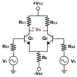
Fig. 1
Inverting & Non inverting Inputs:
In differential amplifier the output voltage vO is given by
VO = Ad (v1 v2)
When v2 = 0, vO = Ad v1
& when v1 = 0, vO = - Ad v2Therefore the input voltage v1 is called the non inventing input because a positive voltage v1 acting alone produces a positive output voltage vO. Similarly, the positive voltage v2 acting alone produces a negative output voltage hence v2 is called inverting input. Consequently B1 is called noninverting input terminal and B2 is called inverting input terminal.
Common mode Gain:
A common mode signal is one that drives both inputs of a differential amplifier equally. The common mode signal is interference, static and other kinds of undesirable pickup etc.
The connecting wires on the input bases act like small antennas. If a differential amplifier is operating in an environment with lot of electromagnetic interference, each base picks up an unwanted interference voltage. If both the transistors were matched in all respects then the balanced output would be theoretically zero. This is the important characteristic of a differential amplifier. It discriminates against common mode input signals. In other words, it refuses to amplify the common mode signals.
The practical effectiveness of rejecting the common signal depends on the degree of matching between the two CE stages forming the differential amplifier. In other words, more closely are the currents in the input transistors, the better is the common mode signal rejection e.g. If v1 and v2 are the two input signals, then the output of a practical op-amp cannot be described by simply
v0 = Ad (v1 v2 )
In practical differential amplifier, the output depends not only on difference signal but also upon the common mode signal (average).
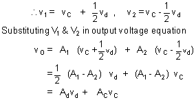
vd = (v1 vd )
and vC = ½ (v1 + v2 )
The output voltage, therefore can be expressed as
vO = A1 v1 + A2 v2
Where A1 & A2 are the voltage amplification from input 1(2) to output under the condition that input 2 (1) is grounded.
The voltage gain for the difference signal is Ad and for the common mode signal is AC.
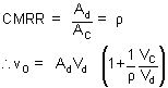
The ability of a differential amplifier to reject a common mode signal is expressed by its common mode rejection ratio (CMRR). It is the ratio of differential gain Ad to the common mode gain AC.
Date sheet always specify CMRR in decibels CMRR = 20 log CMRR.
Therefore, the differential amplifier should be designed so that r is large compared with the ratio of the common mode signal to the difference signal. If r = 1000, vC = 1mV, vd = 1 m V, then
It is equal to first term. Hence for an amplifier with r = 1000, a 1m V difference of potential between two inputs gives the same output as 1mV signal applied with the same polarity to both inputs.