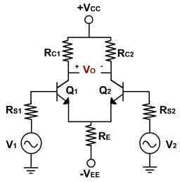
Dual Input, Balanced Output Difference Amplifier:
The circuit is shown in fig. 1 v1 and v2 are the two inputs, applied to the bases of Q1 and Q2 transistors. The output voltage is measured between the two collectors C1 and C2, which are at same dc potentials.
Fig. 1
A.C. Analysis :
In previous lecture dc analysis has been done to obtain the operatiing point of the two transistors.
To find the voltage gain Ad and the input resistance Ri of the differential amplifier, the ac equivalent circuit is drawn using r-parameters as shown in fig. 2. The dc voltages are reduced to zero and the ac equivalent of CE configuration is used.
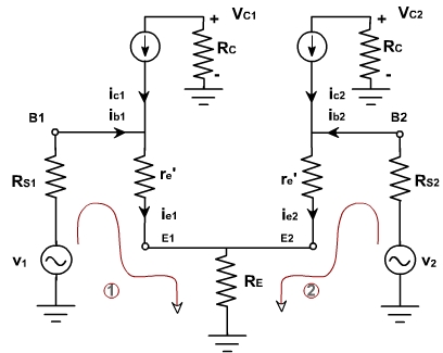
Fig. 2
Since the two dc emitter currents are equal. Therefore, resistance r'e1 and r'e2 are also equal and designated by r'e . This voltage across each collector resistance is shown 180° out of phase with respect to the input voltages v1 and v2. This is same as in CE configuration. The polarity of the output voltage is shown in Figure. The collector C2 is assumed to be more positive with respect to collector C1 even though both are negative with respect to to ground.
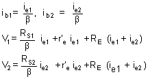
Applying KVL in two loops 1 & 2.
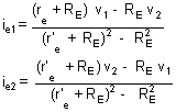
Substituting current relations,
Again, assuming RS1 / b and RS2 / b are very small in comparison with RE and re' and therefore neglecting these terms,
Solving these two equations, ie1 and ie2 can be calculated.
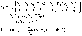
The output voltage VO is given by
VO = VC2 - VC1
= -RC iC2 - (-RC iC1)
= RC (iC1 - iC2)
= RC (ie1 - ie2)
Substituting ie1, & ie2 in the above expression
Thus a differential amplifier amplifies the difference between two input signals. Defining the difference of input signals as vd = v1 v2 the voltage gain of the dual input balanced output differential amplifier can be given by
(E-2)