Dual Input, Balanced Output Differential Amplifier:
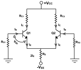
The circuit is shown in fig. 1, v1 and v2 are the two inputs, applied to the bases of Q1 and Q2 transistors. The output voltage is measured between the two collectors C1 and C2 , which are at same dc potentials.
D.C. Analysis:
To obtain the operating point (ICC and VCEQ) for differential amplifier dc equivalent circuit is drawn by reducing the input voltages v1 and v2 to zero as shown in fig. 3.
Fig. 3
The internal resistances of the input signals are denoted by RS because RS1= RS2. Since both emitter biased sections of the different amplifier are symmetrical in all respects, therefore, the operating point for only one section need to be determined. The same values of ICQ and VCEQ can be used for second transistor Q2.
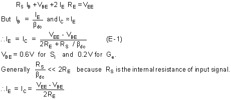
Applying KVL to the base emitter loop of the transistor Q1.
The value of RE sets up the emitter current in transistors Q1 and Q2 for a given value of VEE. The emitter current in Q1 and Q2 are independent of collector resistance RC.
The voltage at the emitter of Q1 is approximately equal to -VBE if the voltage drop across R is negligible. Knowing the value of IC the voltage at the collector VCis given by
VC =VCC IC RC
and VCE = VC VE
= VCC IC RC + VBE
VCE = VCC + VBE ICRC (E-2)
From the two equations VCEQ and ICQ can be determined. This dc analysis applicable for all types of differential amplifier.
Example - 1
The following specifications are given for the dual input, balanced-output differential amplifier of fig.1:
RC = 2.2 kΩ, RB = 4.7 kΩ, Rin 1 = Rin 2 = 50 Ω , +VCC = 10V, -VEE = -10 V, βdc =100 and VBE = 0.715V.
Determine the operating points (ICQ and VCEQ) of the two transistors.Solution:
The value of ICQ can be obtained from equation (E-1).
The voltage VCEQ can be obtained from equation (E-2).
The values of ICQ and VCEQ are same for both the transistors.


