Parameters of OPAMP:
7. Input Voltage Range :
Input voltage range is the range of a common mode input signal for which a differential amplifier remains linear. It is used to determine the degree of matching between the inverting and noninverting input terminals. For the 741C, the range of the input common mode voltage is ± 13V maximum. This means that the common mode voltage applied at both input terminals can be as high as +13V or as low as 13V.
8. Common Mode Rejection Ratio (CMRR).
CMRR is defined as the ratio of the differential voltage gain Ad to the common mode voltage gain ACM
CMRR = Ad / ACM.
For the 741C, CMRR is 90 dB typically. The higher the value of CMRR the better is the matching between two input terminals and the smaller is the output common mode voltage.
9. Supply voltage Rejection Ratio: (SVRR)
SVRR is the ratio of the change in the input offset voltage to the corresponding change in power supply voltages. This is expressed in m V / V or in decibels, SVRR can be defined as
SVRR = D Vio / D V
Where D V is the change in the input supply voltage and D Vio is the corresponding change in the offset voltage.
For the 741C, SVRR = 150 µ V / V.
For 741C, SVRR is measured for both supply magnitudes increasing or decreasing simultaneously, with R3 £ 10K. For same OPAMPS, SVRR is separately specified as positive SVRR and negative SVRR.
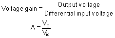
10. Large Signal Voltage Gain:Since the OPAMP amplifies difference voltage between two input terminals, the voltage gain of the amplifier is defined as
Because output signal amplitude is much large than the input signal the voltage gain is commonly called large signal voltage gain. For 741C is voltage gain is 200,000 typically.
11. Output voltage Swing:
The ac output compliance PP is the maximum unclipped peak to peak output voltage that an OPAMP can produce. Since the quiescent output is ideally zero, the ac output voltage can swing positive or negative. This also indicates the values of positive and negative saturation voltages of the OPAMP. The output voltage never exceeds these limits for a given supply voltages +VCC and VEE. For a 741C it is ± 13 V.
12. Output Resistance: (RO)
RO is the equivalent resistance that can be measured between the output terminal of the OPAMP and the ground. It is 75 ohm for the 741C OPAMP.
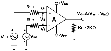
Example - 1
Determine the output voltage in each of the following cases for the open loop differential amplifier of fig. 4:
- vin 1 = 5 m V dc, vin 2 = -7 µVdc
- vin 1 = 10 mV rms, vin 2= 20 mV rms
Fig. 4
Specifications of the OPAMP are given below:
A = 200,000, Ri = 2 M Ω , R O = 75Ω, + VCC = + 15 V, - VEE = - 15 V, and output voltage swing = ± 14V.Solution:
(a). The output voltage of an OPAMP is given by
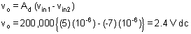
Remember that vo = 2.4 V dc with the assumption that the dc output voltage is zero when the input signals are zero.
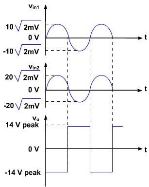
(b). The output voltage equation is valid for both ac and dc input signals. The output voltage is given by
Thus the theoretical value of output voltage vo = -2000 V rms. However, the OPAMP saturates at ± 14 V. Therefore, the actual output waveform will be clipped as shown fig. 5. This non-sinusoidal waveform is unacceptable in amplifier applications.
Fig. 5
13. Output Short circuit Current :
In some applications, an OPAMP may drive a load resistance that is approximately zero. Even its output impedance is 75 ohm but cannot supply large currents. Since OPAMP is low power device and so its output current is limited. The 741C can supply a maximum short circuit output current of only 25mA.
14. Supply Current :
IS is the current drawn by the OPAMP from the supply. For the 741C OPAMP the supply current is 2.8 m A.
15. Power Consumption:
Power consumption (PC) is the amount of quiescent power (vin= 0V) that must be consumed by the OPAMP in order to operate properly. The amount of power consumed by the 741C is 85 m W.