Series regulator with Current Pre-regulator
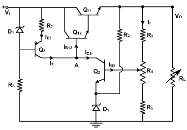
The circuit of fig. 1 is an improved version of series voltage regulator discussed in previous lecture. Besides Q1 being replaced with a current regulator circuit. The function of D2, R6, R7, and Q3 is to establish and maintain a constant I1.
Fig. 1
The circuit works this way :- I1 is the collector current of Q3, and hence it is also approximately equal to IE3. The voltage at the base of Q3 relative to V1 is held at a constant level by D2; current through R6 is selected to keep D2 in breakdown and to yield the proper temperature coefficient. Should I1 rise, IE3 will also rise, increasing the voltage across R1. This reduces VEB3, which in turn reduces IE3 and I1. Thus I1 is regulated and remains fairly constant even if there are changes in the unregulated input.
One disadvantage of this circuit is that a larger input voltage is required to supply the various voltage drops between Vi and Vo. In this case Vi must supply Vo plus the two VEB drops of Q11 and Q12 (which takes us to point A), plus the collector-base bias for Q3 (which takes us to the base Q3), plus the Zener voltage for D2.
Power Supply Using IC Regulator (Three-Terminal Regulator)
Monolithic integrated circuits have greatly simplified the design of a wide variety of power supplies. Using a single IC regulator and a few external components, we can obtain excellent regulation (on the order of 0.01%) with good stability and reliability and with overload protection.
IC regulators are produced by a number of manufacturers. The IC regulator improves upon the performance of the Zener diode regulator. It does this by incorporating an operational amplifier. In this section, we present basic design considerations for IC regulators. These techniques are useful in the design of power supplies for a variety of low power applications. We consider the internal theory of operation of these and other three-terminal voltage regulators in the current section. These products vary in the amount of output current. The most common range of output current is 0.75 A to 1.5 A (depending on whether a heat sink is used).
Fig. 2
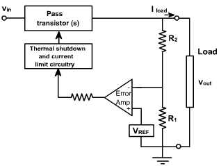
The functional block diagram of fig. 2 illustrates the method of voltage regulation using this series regulator. The name series regulator is based on the use of a pass transistor (a power transistor) which develops a variable voltage which is in "series" with the output voltage. The voltage across the pass transistor is varied in such a manner as to keep the output voltage constant.
A reference voltage, VREF, which is often developed by a Zener diode, is compared with the voltage divided output, vout. The resulting error voltage is given by
The error voltage v e is amplified through a discrete amplifier or an operational amplifier and used to change the voltage drop across the pass transistor. This is a feedback system which generates a variable voltage across the pass transistor in order to force the error voltage to zero. When the error voltage is zero, we obtain the desired equation by solving equation (Equ-1) for vout .
Thermal shutdown and current-limit circuitry exists between the error amplifier and the pass transistor. This circuitry protects the regulator in case the temperature becomes too high or an inadvertent short circuit exists at the output of the regulator.