Example 1
The following data apply to a voltage regulator circuit shown in fig. 1 Unregulated input: Vi = 15 to 20V
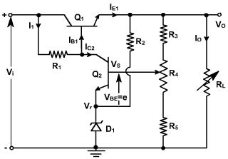
|
Fig. 1 |
Solution
(a). Since RL = VO / IO, we can write
The maximum load current is zero; therefore the load resistance is anywhere from 100Ω to an open circuit.
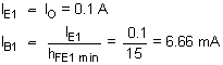
(b). The base current of Q1 is IE1 (hFE1 + 1), where IE1 is the sum of load current IO, current through the sampling network, and current through R2. Usually IO is the largest component involved; therefore
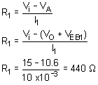
(c). R1 should supply the maximum current required by the base of Q1. This is 6.66 mA; however, it is a good practice to increase it by about 50 percent to provide a safety margin. We therefore select R1 on the basis that its current must never drop below 10 mA:
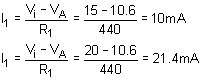
(d). The extreme values of I1 are determined using the extreme values of Vi:
(e).
(f). Worst-case power dissipation for Q1 occurs when both the voltage and current are maximum. Normally the collector-base junction dissipates the most power, since its voltage is much greater than VBE; however, the total transistor dissipation involves both junctions. This can be approximated as follows:
Voltage across Q1: VCE1 = Vi VO
Current through Q1: IC1 ≈ IE1 ≈ IO
PE1 ≈ (Vi VO) (IO)
PD1≈ (20 10) (0.1) = 1 W(g). Q2 does not handle large currents as Q1 does; therefore its power dissipation is relatively low:
PD2 = (VCE2) (IC2)
Both VA and Vr are relatively constant; therefore VCE2 is also constant:
VCE2 = VA Vr = VO + VEB1 Vr
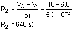
VCE2 = 10 + 0.6 6.8 = 3.8 VThe maximum value of IC2 is approximately equal to I1 = 21.4 mA; we, therefore, have
PD2 ≈ VCE2 IC2
PD2 ≈ 4(21.4 x 10⁻³) = 81.5 mWNote that the current through R1 in this example does not remain constant; in fact, it can vary between 10 and 21.4 mA, a total range of 11.4 mA. The regulator would perform much better if I1 were regulated.