2.2 MOS Device Current -Voltage Equations
This section first derives the current-voltage relationships for various bias conditions in a MOS transistor. Although the subsequent discussion is centred on an nMOS transistor, the basic expressions can be derived for a pMOS transistor by simply replacing the electron mobility ![]() by the hole mobility
by the hole mobility ![]() and reversing the polarities of voltages and currents.
and reversing the polarities of voltages and currents.
As mentioned in the earlier section, the fundamental operation of a MOS transistor arises out of the gate voltage VGS (between the gate and the source) creating a channel between the source and the drain, attracting the majority carriers from the source and causing them to move towards the drain under the influence of an electric field due to the voltage VDS (between the drain and the source). The corresponding current IDS depends on both VGS and VDS .
2.2.1 Basic DC Equations
Let us consider the simplified structure of an nMOS transistor shown in Figure 2.8, in which the majority carriers electrons flow from the source to the drain.
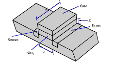
Fig 2.8: Simplified geometrical structure of an nMOS transistor
![]() CLICK ON THE LEFT IMAGE TO VIEW IT'S ENLARGE PICTURE
CLICK ON THE LEFT IMAGE TO VIEW IT'S ENLARGE PICTURE