Module 3 : Fabrication Process and Layout Design Rules
Lecture 13 : Layout Design Rules
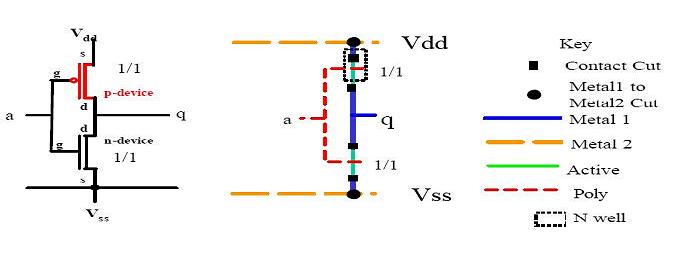
13.4 Stick Diagrams
Another popular method of symbolic design is "Sticks" layout. In this, the
designer draws a freehand sketch of a layout, using colored lines to represent the
various process layers such as diffusion, metal and polysilicon .Where polysilicon
crosses diffusion, transistors are created and where metal wires join diffusion or
polysilicon, contacts are formed.
This notation indicates only the relative positioning of the various design
components .The absolute coordinates of these elements are determined
automatically by the editor using a compactor. The compactor translates the design
rules into a set of constraints on the component positions ,and solve a constrained
optimization problem that attempts to minimize the area or cost function.
The advantage of this symbolic approach is that the designer does not have to
worry about design rules, because the compactor ensures that the final layout is
physically correct. The disadvantage of the symbolic approach is that the outcome of
the compaction phase is often unpredictable. The resulting layout can be less dense
than what is obtained with the manual approach. In addition, it does not show exact
placement, transistor sizes, wire lengths, wire widths, tub boundaries.
For example, stick diagram for CMOS Inverter is shown below.