| |
9.2.1 Magnetron Sputtering
Sputtering is one of the effects in glow discharge processes when a surface is bombarded by energetic particles. In this process the target atoms are ejected by the bombardment of energetic species (usually inert gas ions) on it, as shown in Figure 9.2. The sputtered atoms travel through the plasma and undergo many collisions with the plasma species (electrons, neutrals, gas ions, and metals ions) and subsequently deposit on a strategically placed substrate. The substrate can be heated depending upon the nature of the deposition. Sputtering process can employ dc or rf power depending upon the electrical conductivity of the target. DC power can be used only for conducting targets where rf power can be used for both conducting and insulating targets. Usually a magnetic field (use of magnetron target) is employed to enhance the efficiency of plasma utilisation and sputter efficiency. This happens due to increased electron residence time in the plasma, improving the ion collision probability and thus larger discharge currents. Sputtering process using a magnetron is called magnetron sputtering. A complete description of glow discharge processes and their application to sputtering process can be found elsewhere.11
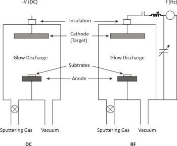 |
| Figure 9.2 Schematic diagram of DC and RF sputtering process |
Reactive sputtering can be used to prepare alloys or compounds, solid solutions, or a mixture. Reactive sputtering in a mixture of oxygen and argon has been a very important process for the deposition of oxides since the 1970s. Among one of the earlier studies, a mixture of argon (Ar) and oxygen (O2) was used to deposit SiO2 films from elemental Si target by reactive sputtering.12 Application of RF sputtering facilitated the use of an oxide as the starting material and target, but given the variation in the sputter yields of different elements, the resulting films were not found to be stoichiometric.
Growth of oxides by sputtering involves different regimes depending upon the sputtering conditions. Work has shown that the nature of growth species changes from atomic to molecular as the sputtering gas pressure increases.13 One major problem encountered in the sputtering of oxides is the resputtering of the growing film by negative ions and reflected neutrals14,15, leading to morphological changes e.g. formation of various features such as pits, ripples, cones and craters on the film surfaces. Presence of these morphological changes was found to be dependent on a number of factors including deposition rates, flux and energy of bombarding ions, and the average angle of incidence of bombarding ions. These studies also predicted that resputtering can be minimized by thermalizing (reducing the energy of energetic species originating from the target) the energetic species in the plasma either by sputtering in high pressure environment or by off-axis sputtering. The issue of whether to use an oxide target or an elemental target is quite complex. Some of the considerations in selecting a particular target are target purity, deposition rates, and stoichiometry related issues.
Interdependence of various parameters makes this process quite complex. The main issues which are to be addressed are stoichiometry control, epitaxy, nature of the substrates (can involve use of buffer layers), and oxygen activity during the deposition.16 It has been studied that given the condition that all the factors, particularly temperature, partial pressure of oxygen and total pressure, are within reasonable control, sputtering can produce films with good structural quality and good composition control within an accuracy of 0.1%.17 Highly oriented oxide films can be grown with controlled stoichiometry and properties as shown by various groups for high Tc superconducting films18,19 and ferroelectric films.20 However, one of the major drawbacks is slow deposition rate which makes this process quite expensive.
.
| 11B. Chapman, Glow Discharge Processes, John Wiley & Sons. (1980) |
| 12J.C. Erskine and A. Csahati, J. Vac. Sci. Tech., 15, 1823 (1978) |
| 13Y.M. Boguslavsky, Supercond. Sci. Tech., 4, 149 (1991) |
| 14S.M. Rossanagel and J.J. Cuomo, in ‘Thin Film Processing and Characterisation of High Temperature Superconductors’, eds. Harper J.M.E., Colton R.J., and Feldman L.C., American Institute of Physics Conf. Proc., 165, AIP, NY, 106 (1988) |
| 15D.J. Kester and R. Messier, J. Mater. Res., 8, 1928 (1993) |
| 16R.E. Somekh, in ‘Physics and Materials Science of High Temperature Superconductors’, Dordrecht, The Netherlands, Kluwer Academic Publishers, 327 (1990) |
| 17E.J. Tomlinson, Z.H. Barber, G.W. Morris, R.E. Somekh, and J.E. Evetts, IEEE Trans. Appl. Magn. 2, 2530 (1988) |
| 18J. Geerk, G. Linker and O. Meyer, Mater. Sci. Rept., 4, 193 (1989) |
| 19G. Linker, X.X. Xi, O. Meyer, O. Li, and J. Geerk, Solid State Commun., 69, 249 (1989) |
| 20O. Auciello, A.I. Kingon, and S.B. Krupanidhi, MRS Bulletin, June, 25 (1996) |
|