Voltage response in piezoelectric patch for Configuration 1
Figure 25.3(a) shows the voltage response in the elements when delamination is considered in element 1. A drop in voltage from 0.31V to 0.30V is predicted. Since element 1 is not receiving any load, a localized stress redistribution will cause modified voltage responses in elements located close to it.
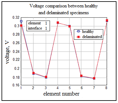
Figure 25.3 (a) Voltage profile for damage in element 1 of interface 1
Figures 25.3(b) to 25.3 (f) show the voltage responses when delaminations are assumed in elements 2, 3, 4, 5 and 8 respectively. Elements 2 and 3 (and their corresponding symmetric pairs 7 and 6) show little change in response due to delamination [Figures 25.3(b) and (c)].
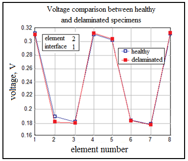
Figure 25.3(b) Voltage profile for damage in element 2 of interface 1
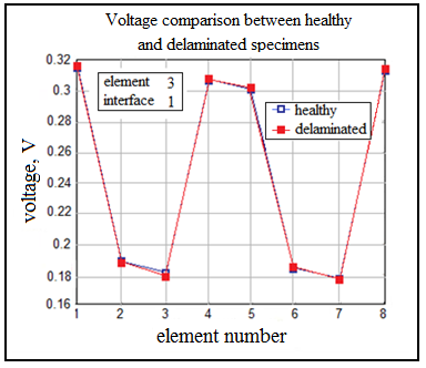
Figure 25.3(c) Voltage profile for damage in element 3 of interface 1
|