| Single-stage Generator Circuit |
- Two basic circuits for single-stage impulse generator are shown in Fig. 28.1 (a) and (b).
- The capacitor C1 is charged slowly from a dc source until the spark gap G breaksdown and discharges upon C2, the load capacitor over the resistors R1 and R2.
- This spark gap acts as a voltage-limiting and voltage sensitive switch.
- An economic limit of the charging voltage U 0 is about 200 to 250 kV. Too large diameter of the identical spheres would otherwise be required to achieve weakly nonuniform field between the spheres for longer gap distances.
- The resistors R1, R2 and the capacitance C2 form the wave-shaping network. R1 primarily controls the wave front time T1. R2 over which the capacitor discharges, essentially controls the wavetail time T2.
- The capacitance C2 represents the load, i.e. the object under test as well as all other capacitive elements which are in parallel to the test object (measuring devices; additional load i.e., capacitor to avoid large variations of T1 / T2, if the test objects are changed).
- No inductances are assumed so far, and are neglected in the first fundamental analysis, necessary to understand multi-stage generators.
- This approximation is in general permissible, as the inductance of all elements has to be kept as low as possible.
- From the output voltage efficiency point of view, the circuit shown in Fig 20.1(b) is more efficient compared to the circuit in (a). It is because the resistances R1 and R2 do not form a voltage dividing system in (b). It is this more efficient circuit which has found wider application. Hence for the analysis, this circuit in Fig 20.1(b) will be considered.
Before starting the analysis, one of the most significant parameter of impulse generators must be described. It is the energy rating of the impulse generator, given by;
|
 (28.1) |
|
Fig 28.1 Single-stage impulse generator circuits (a) and (b). C1 : charging capacitor. C2: load capacitance. R1 :Wave front resistance. R2 : Wave tail resistance. (c) Laplace Transformed circuit.
|
- C1should be always chosen much larger than C2, hence it determines the cost of the generator.
- For the analysis we may use the Laplace transform circuit shown in Fig. (28.1(c)) which simulates the boundary condition, that when t ≤ 0, C1 is charged to U 0 and for t > 0 this capacitor is directly connected to the waveshaping network.
- For the efficient circuit in Fig. 28.1(b), the output voltage is given by,
|
| |
By substitution we find
|
 (28.2) (28.2) |
where
|
 (28.3) (28.3) |
| |
From the transform tables the following expression in the time domain can be obtained:
|
 (28.4) (28.4) |
where α1 and α2are the roots of the equation s2 + as + b = 0, or
|
 (28.5) (28.5) |
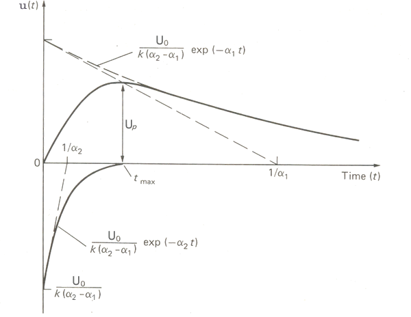
- The output voltage u(t) is therefore the superposition of two exponential functions of different signs.
- According to eqn. (28.5), the negative root leads to a larger time constant 1/α1 than the positive one, which is 1/α2
- A plot of the expression [eqn. (28.4)] is shown in Fig. 28.2.
|
 |
Fig 28.2 The impulse voltage wave components according to the circuit equation |
| |
- The voltage efficiency is defined as,
|
 (28.6) (28.6) |
- Up , the peak value of the output voltage as indicated in Fig. 28.2. Obviously this value is always smaller than U0.
- Time for the voltage u(t) to rise to its peak value can be determined by equating:
|

therefore
 (28.7) (28.7)
|
- Substituting this equation in eqn. (28.4), the efficiency can be found,
|
 (28.8) (28.8) |
- By substitution, the voltage efficiency for the condition C2 << C1 is obtained as;
|
 (28.9) (28.9) |
- Fig. 28.3 shows the voltage efficiency of the circuit with increasing load capacitance.
|
|
Figure 28.3 Voltage efficiency factor with increasing capacitance ratio C2/C1 for lighting impulse. |
| |