| |
POWER4 caches
- Private L1 instruction and data caches (on chip)
- L1 icache: 64 KB/direct mapped/128 bytes line
- L1 dcache: 32 KB/2-way associative/128 bytes line/LRU
- No M state in L1 data cache (write through)
- On-chip shared L2 (on-chip coherence point)
- 1.5 MB/8-way associative/128 bytes line/pseudo LRU
- For on-chip coherence, L2 tag is augmented with a two-bit sharer vector; used to invalidate L1 on other core’s write
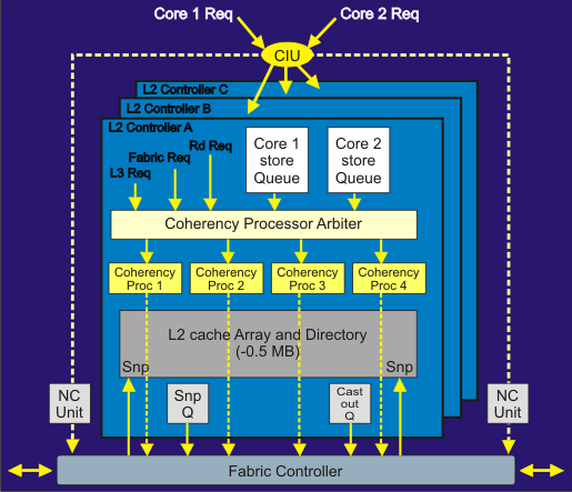
- Three L2 controllers and each L2 controller has four local coherence units; each L2 controller handles roughly 512 KB of data divided into four SRAM partitions
- For off-chip coherence, each L2 controller has four snoop engines; executes enhanced MESI with seven states
POWER4 L2 cache
|
| |
| |
| |
| |
| |
| |
| |
| |
| |
| |
| |
| |
| |
| |
|
|
|
|