Minimization of channeling:
One way to prevent channeling is to hold the wafer at an angle. This can prevent channeling, but it can cause other issues like increase in transverse struggle and also cause shadow as shown in the figure.
.jpg)
Figure 7.9 Schematic illustrating effect of holding the wafer at an angle (to minimize channeling)
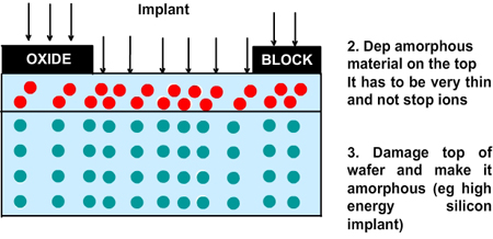
Too much of an angle can also be a problem. Another way is to deposit amorphous material on the top. It has to be very thin so that it will not stop the ions, but an amorphous material will make sure that the incoming ion does not see a very uniform structure with gaps.

Figure 7.10 Schematic illustrating depositing amorphous material or damaging the surface of wafer, to minimize channeling
The third option is, instead of depositing amorphous material, just damage the top of the wafer; that is, make it amorphous using high-energy silicon implant. The fourth choice is to increase the temperature and reduce the channel cross-section. |