Semiconductor Heterojunction .
For faster transit time, RC should be decreased. This is used in making HBTs/HEMTs.
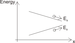
Two semiconductors with two different bandgaps can be grown one on top of the other or a material can be grown with variable band as shown in Fig 14.1 For a constant bandgap semiconductor electrons and holes move in opposite direction with the application of the electric field. In a heterostructure as shown both can move same direction !!
Material that has a higher Band Gap is denoted by  and that having lower Band Gap is denoted by n or p as usual. So we can have pN, nP or p+ N heterojunction. and that having lower Band Gap is denoted by n or p as usual. So we can have pN, nP or p+ N heterojunction.
Few applications of heterostructures are HBT, diode laser, LED, Photodetector, Quantum well devices, solar cells.
The materials that are grown together mus be latticed matched. Few lattice matched compound semiconductors are
 and and  and and  and and  on GaAs. on GaAs.
 is basically solid solution (alloy) of Al, As and GaAs with no interface traps is basically solid solution (alloy) of Al, As and GaAs with no interface traps
We use molecular beam Epitaxy (MBE) or metal organic chemical vapour deposition (MOCVD) to growth these structures. Liquid phase epitaxy is also used.
Calibration is done with Reflection high energy electron diffraction (RHEED)
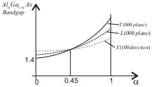
For  Bandgap minimum remains at Bandgap minimum remains at  keeping the alloy as direct bandgap and keeping the alloy as direct bandgap and
for  Bandgap minimum occurs at X making the material indirect bandgap as shown in Fig 14.2 Bandgap minimum occurs at X making the material indirect bandgap as shown in Fig 14.2
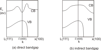
The energy diagram of the direct and indirect bandgap materials are shown in Fig 14.3
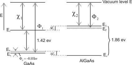
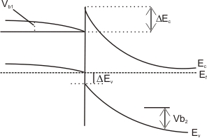
Now consider an abrupt p-n junction p type GaAs and N type AlGaAs
First we draw their energy band diagram side by side as shown in Fig 14.4 then the two energy band diagrams are brought in contact, keeping the E F same on both sides as shown in Fig 14.5 Electron flows from N side to  side and holes from p side to N side and a depletion region is formed. side and holes from p side to N side and a depletion region is formed.
Fig 14.4
Fig.14.5
Hence at thermal equilibrium Fermi level lines up on both sides.
Hence we get

We note that the two sides has two different permittivity.
The Poisson Equation are
Now theE field is zero at  and and 
Thus
and
The potential profile is obtained by integrating  and assuming and assuming  , the potential is given by , the potential is given by
The built-in potential on the p-side is
And the built-in potential on the N-side is
The electric flux density is continuous across the jiunction, hence
Also  , (the charge conservation relationship) , (the charge conservation relationship)
Considering all these we can show that for applied 
Also  |
So,
|