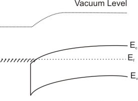
When a metal-semiconductor junction is formed such that the carries see a barrier to flow from one terminal to the other,it as called a schottky barries ,as shown in 12.6.
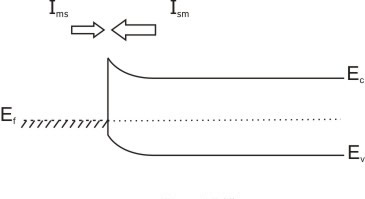
When the Schottky diode is forward biased (negative with respect to metal) by a voltage  the barrier for electrons in Semiconductor decreases from the barrier for electrons in Semiconductor decreases from  to to  . More electrons flows from Semiconductor to metal . More electrons flows from Semiconductor to metal  increases greatly as shown in Fig 12.6 increases greatly as shown in Fig 12.6
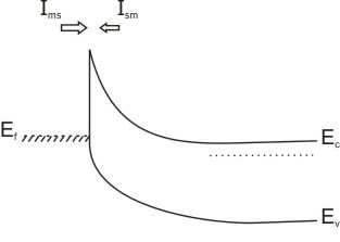
But  remains unchanged because no voltage drop across metal and remains unchanged because no voltage drop across metal and  remains unchanged. Reverse bias drops across semiconductor increasing the barrier remains unchanged. Reverse bias drops across semiconductor increasing the barrier  to to  where V R is negative now, where V R is negative now,  decreases more but decreases more but  remains almost unchanged. Small reverse current flows from Semiconductor to metal as shown in Fig 12.7 remains almost unchanged. Small reverse current flows from Semiconductor to metal as shown in Fig 12.7
Now suppose we have a semiconductor. with  as shown in Fig 12.4 as shown in Fig 12.4
No depletion layer is formed in Semiconductor, no barrier exists in semiconductor or in metal.
Metal +n-type is rectifying for  and non rectifying and non rectifying 
Opposite is true for p-type  rectifying contact otherwise ohmic as shown in Fig12.5 rectifying contact otherwise ohmic as shown in Fig12.5
For rectifying contact
 Maximum Maximum  field occurs at field occurs at
|
The space charge per unit area
Or  . Thus if . Thus if  is constant throughout is constant throughout
Fig10.5 ps |
|