PIN Diode
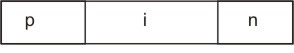
In PIN diode the i region is sandwiched between the p and n region as shown in Fig 11.5
The i-region is either a high resistivity  layer. layer.
PIN diodes are fabricated by
-epitaxial process
-Diffusion of p and n in high resistability substrate
-ion drift method
The concentration, charge density and electric field profiles are shown in Fig 11.6
PIN diodes are used widely in microwave wave circuits such as microwave switch with constant depletion layer and high power.
The switching speed 
Where W is the total depletion region width and  is the saturation velocity across i region. is the saturation velocity across i region.
In addition the PIN diode can be used as
-variable attenuator by varying device resistance that change approximately likely with forward current
-Modulate signals up to GHz range.
-Photo detection of internal modulated light in reverse bias.
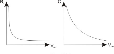
Under Riverse Bias the junction capacitance is
and the series resistance is
Where  is the i-region resistance and is the i-region resistance and  is the contact resistance. is the contact resistance.
The reverse bias current is
Where  is the ambipolar life time. The I-V characteristics is shown in Fig 11.7 is the ambipolar life time. The I-V characteristics is shown in Fig 11.7
|