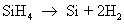
There are four major chemical sources of silicon for commercial epitaxial deposition: (1) silicon tetrachloride (SiCl4), (2) trichlorosilane (SiHCl3), (3) dichlorosilane (SiH2 Cl2) and (4) silane (SiH4). The over-all reaction for silicon epitaxy by silane reaction may be written as follows:
The growth of an epitaxial layer over the substrate offers some advantages. By growing a lightly doped epi layer over a heavily-doped silicon substrate, a higher breakdown voltage across the collector-substrate junction is achieved while maintaining low collector resistance. Lower collector resistance allows a higher operating speed. By fabricating the CMOS device on a very thin (3-7 µm) lightly doped epi layer grown over a heavily-doped substrate, latch-up occurrence is minimized. Aside from improving the performance of devices, epitaxy also allows better control of doping concentrations of the devices. The layer can also be made oxygen- and carbon-free. The disadvantages of epitaxy include higher cost of wafer fabrication, additional process complexities, and problems associated with defects in the epi layer.
In this section we have studied about the crystal structure, how it was grown and converted to wafers. The next section discusses the importance of wafer cleaning and different methods used to remove contaminations.