Contact printing :
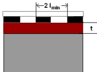
Resist is in contact with the mask. 1:1 magnification is achieved. The advantages of this method are inexpensive equipment, faster process, the entire wafer is exposed at once and moderately high resolution is achieved; ~0.5 um or better but limited by resist thickness. The diffraction effect is minimized as the gap is between mask and wafer is zero.
Fig. 3.56 : Model of a contact printing scheme