- PN junction diodes are used in a wide variety of applications, with
each application taking advantage of a different set of diode's characteristics.
A few of the applications along with the diode characteristics on which they are base are listed below:
Application Mode of Operation Principle Switching circuits Forward and Reverse bias with time varying signals Rectification Photodetectors Reverse bias with time varying signals Sensitivity of reverse current to carrier generation Solar Cells Forward bias with constant excitation Sensitivity of diode current to carrier generation Mixers Forward bias with time varying excitation Nonlinear diode characteristics
Let us consider applications where rectifying characteristics of the PN junction diodes is exploited. In these cases, the following characteristics are of interest:
(i) Maximum forward current that
can flow through the device beyond
that
can flow through the device beyond
which the forward ON voltage begins to increase linearly rather than logarithmically with current.
(ii) The reverse leakage current at
small reverse bias
at
small reverse bias
(iii) Breakdown voltage BV
(iv) Reverse recovery time
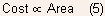
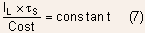
The desired diode characteristics have to be obtained at the least cost (C) possible
Let us consider the tradeoffs among these diode characteristics for a wide base
diode
Th max. forward current limited by onset of high level injection is determined by the
doping in the lightly doped region :
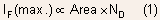
- This breakdown voltage can be expressed as

- The reverse leakage current is proportional to
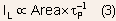
- The reverse recovery is proportional to

- Finally, the cost of diode is proportional to silicon area used so
that
The equations listed above can be used to obtain the following expressions
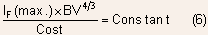
- This expression describes a very important tradeoff among the max.
current rating, breakdown voltage and cost of a diode
- It shows that an increase in forward current can only be obtained
either at the expense of a lower breakdown voltage or increased cost
due to use of larger Silicon area
.
- The expression also shows that high voltage, high current diodes are
likely to be the most expensive diodes.
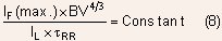
Another expression describing another important tradeoff can be written using the equations listed earlier:
- This expression shows that an improvement in switching performance
can be obtained either at the expense of increased leakage current or
a reduced cost. The reduced cost or smaller diode area implies either
a lower forward current or a lower breakdown voltage according to Eq.
(6)
- It is interesting to see how breakdown voltage can be traded with
switching speed. A reduction in recombination lifetime through say addition
of suitable impurities will also increase leakage current. This can
be countered by decreasing diode area which however will lead to reduced
forward current rating unless doping is increased. This will lead to
a reduced breakdown voltage.
- The breakdown voltage and reverse recovery are also related together
in more direct manner. Regions which have higher doping also have a
lower recombination lifetime so that a lower breakdown voltage diode
is likely to have lower lifetime and better switching speeds.
The two tradeoff expressions can also be combined to obtain another expression shown below:
- The expression above shows why a single diode cannot meet the needs
of diverse applications. Different applications put different demands
on forward current, breakdown voltage etc which can only be obtained
through separate designs.
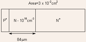
Example 6.1 Design a wide base diode with a breakdown voltage
Solution: We shall take
Taking the critical field
To be on the safe side , we take
The maximum current handling capability is determined by the onset of high level injection effects.
The maximum current density is
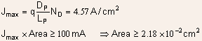
Again to be on the safe side, we take
To be considered as wide base diode, the width of N-region should be several times the diffusion length which is 28µm. so we take
Example 6.2 Design a narrow base diode with similar specifications. Comment on the advantages of the narrow base over the wide base diode.
Solution : As before, we take
From this we obtain,
The maximum current density now is
Again, to be on the safe side, we take
Advantages: The area required is an order of magnitude better . Further the transit time of diode now is