- The I-V model derived earlier is valid under steady
state conditions when charges, currents and voltages are static. To
determine the behavior of the PN junction under time varying excitation,
we start from the continuity equation where time explicitly comes into
picture:

where A is the area of the device. Integrating this equation across the depletion region gives:

By virtue of depletion approximation, the last term is zero. The second term can also be neglected because it is much smaller than the first term ;
while
;
while 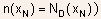

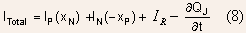
The net current can be expressed as:

The first three are familiar terms. The last term can be rewritten by noting that the junction depletion charge can be expressed as:
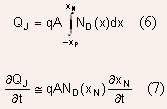
Therefore, the net current can be expressed as:
The last term represents the current due to time variation of the junction depletion charge The current due to variation of depletion charge can be expressed as:

where the voltage across the junction

where the voltage across the junction
where is
the junction depletion capacitance. An expression for junction dV capacitance
can be easily obtained using the depletion approximation and will be
discussed later.
is
the junction depletion capacitance. An expression for junction dV capacitance
can be easily obtained using the depletion approximation and will be
discussed later.
The net current can now be expressed as:

Let us next look at he minority carrier currents. Under low level injection approximation, they can be assumed to be diffusive so that:

As for the static case, the computation of these currents requires determination of minority carrier profiles, which in turn requires solution of continuity equation. For the computation of p(x), the hole continuity equation in N-region has to be solved:

- This is where the other major difference between static
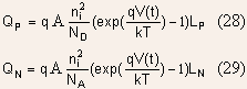
and time varying characteristics comes. Unlike the static case,
 is
no longer zero .
is
no longer zero .
For low level injection condition: so
that integration of hole continuity equation across the N-region for
a long base diode gives:
so
that integration of hole continuity equation across the N-region for
a long base diode gives:

Far away from the junction, the hole current would be zero so that:

 is
the diffusion charge due to excess holes stored in the N-region. The
first term in the expression above is also present under static conditions
and represents the current due to recombination of injected holes. The
second term represents the current due to time variation of stored excess
hole charge
is
the diffusion charge due to excess holes stored in the N-region. The
first term in the expression above is also present under static conditions
and represents the current due to recombination of injected holes. The
second term represents the current due to time variation of stored excess
hole charge
For the N-side also a similar expression can be written:

With these expressions for minority carrier currents, the total current after neglecting the SCR recombination current, can be expressed as:

- This representation of the diode's behavior is known
as the Charge Control model. The operation of many semiconductor devices
can be conceptualized as a two step process where the applied voltage
modulates the charge within the device, which then modulates the current.

Just as the term can be expressed as
  ,
similarly, the time variation of
,
similarly, the time variation of
diffusion charge can be expressed as:

- The change in diffusion charge with the applied bias
can be represented by a diffusion capacitance defined as

The total device current can now be expressed as

The first two terms represent current due to recombination in N and P-regions respectively, while the last two represent the current due to charge/discharge of junction and diffusion capacitances.
- To use the above equation, a relationship between the
diffusion charges (and capacitances) and the applied bias is needed.
This again requires solution of the continuity equation with the boundary
condition that

- The continuity equation being a partial differential
equation is often difficult to solve analytically. It is often assumed
that the minority carrier profile under transient conditions has the
same form as that under static conditions. In other words:

- This assumption, known appropriately as the Quasi-static
assumption is frequently invoked in analysis of other semiconductor
devices as well in order to obtain a simplified solution. The range
of validity of this assumption will be discussed a little later.
Use of quasi-static assumption allows the diffusion charges to be expressed as
The component of current due to minority carrier diffusion and recombination has exactly the same form now as under static conditions:

The diffusion capacitance can be expressed as:

For the simplified case: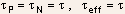
The final model of current under quasi-static approx. is:

The first term is the conventional diode current, while the last two terms are due to capacitive effects.
- The expression for total current shows that current
under dynamic conditions is the sum of a current which is identical
in form to the static current and currents due capacitances in the device.
- The development of a dynamic model under quasi-static
conditions therefore involves only development of a capacitance model
of the device. This model is developed by assuming that charge distribution
has a form as under static conditions.
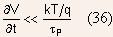
The validity of the quasi-static assumption for the PN junction diode can be checked by revisiting the continuity equation:

The quasi-static assumption would be valid ifis
much smaller than either of the two
terms on the right:

Taking ,
we obtain the condition for validity of the quasi-static assumption
as:
,
we obtain the condition for validity of the quasi-static assumption
as:
Similarly, for the N-side

For the excitation one
obtains an upper limit on the excitation frequency:
one
obtains an upper limit on the excitation frequency:

If the amplitude of the sinusoidal excitation is kept less than the thermal voltage, then quasi static approximation gives reasonable result for frequencies less than
- The quasi-static assumption breaks down when the voltage across the
diode is abruptly switched as shown below:

The figure above shows a schematic representation of the current waveform that may be experimentally observed:
For the sake of simplicity, we shall assume a wide-base
diode The charge control model gives:
wide-base
diode The charge control model gives:

The diffusion capacitance, as will be shown later, is much larger than the junction capacitance, so that the last term in the expression above can be ignored.
For ,
when the diode is in steady state:
,
when the diode is in steady state:

After the voltage is switched:

The reverse current removes the excess charge stored in the N-region and continues to flow till all charge is removed.
- Even though quasi-static approx. is not strictly valid here, nevertheless
let us use it to get an estimate of the reverse recovery time.
The QS approx. implies that: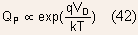
- Because of the exponential dependence of charge on diode voltage,
the change in diode voltage as the diffusion charge falls from 100%
to say 10% of its initial value is less than 60mV and can therefore
be neglected.
- Therefore, the diode voltage and hence the reverse current can be
practically assumed to be constant over the entire reverse recovery
period.
This allows the solution of the differential equation to be written as:

The total time for which the diode remains conducting despite the applied reverse bias can be obtained by substituting in
the above expression
in
the above expression

The expression shows that the charge storage time is
directly proportional to the minority carrier lifetime.
is
directly proportional to the minority carrier lifetime.
The accuracy of this expression is questionable because the quasi-static approx. as mentioned earlier is not valid here because of the abrupt reversal in applied voltage.
- The quasi-static approx. implies that the form of minority carrier
profile remains the same as under static conditions even though the
junction voltage is time varying. The charge decay process is therefore
modeled as shown below:

- The consequence of such a profile is that it predicts almost constant
reverse current throughout the transient unlike what happens in reality.
Because the current is flowing in the reverse direction at the junction, the expression for diffusion current demands that the slope of the minority carrier profile at the junction be positive and not negative as under static conditions.

The actual minority carrier profile on the N-side during the transient actually looks more like that shown below:
The reverse transient can be broken into two phases:

(i) Constant reverse current phase
(ii) Decaying current phase
- During the constant current phase, the minority carrier density at
the depletion edge is non zero:
.gif) >0.
>0.
In this situation, the reverse current is primarily determined by the external resistor because
(and therefore the diffusion current) can adjust to any value without appreciable change in the diode voltage. This phase of the transient is therefore characterized by a constant reverse current.
- When falls
to zero, the minority charge does not reduce to zero as was assumed
to happen in the quasi-static case.
There is still a large fraction of stored charge that has to be removed. The reverse current under these conditions is unaffected by the diode voltage becauseis
already zero and cannot be further altered. As a result, current is
now determined by the dynamics of the internal hole distribution.
- The peak hole density decreases with time causing the reverse current
also to decrease. This part of the transient is known as the fall time
delay.
An analytical solution of the time dependent continuity equation can be obtained to determine the values of the storage and fall times but for simplicity only the results will be stated here and compared with that obtained using quasi-static assumption.

- It can be seen that despite the approximation, the estimate of reverse
recovery time using quasi-static approx. is quite accurate if the ratio
of forward and reverse current is not too low.
Junction Capacitance
The junction capacitance in the preceding discussion was defined as

To determine an expression for junction capacitance, the incremental change in
response to incremental change
in
response to incremental change  needs
to be computed.
needs
to be computed.
- As a result of the change in junction voltage, an extra charge
 will
be created on the N-side and an equal but opposite charge
will
be created on the N-side and an equal but opposite charge on
the P-side as illustrated in the Figure:
on
the P-side as illustrated in the Figure:

The incremental increase in electric field within the junction as a result of these extra charges is

The corresponding change in junction voltage is:

For a uniformly doped PN junction, the depletion approx. gives:

where is
the zero bias junction capacitance. The model derived for junction
is
the zero bias junction capacitance. The model derived for junction
capacitance is based on depletion approximation. The model works well in reverse bias but tends to overestimate the junction capacitance at high forward bias.
For the junction capacitance per unit area is
Let us compare this value with the diffusion capacitance:
 for a wide base
junction.
for a wide base
junction.
For ,
this turns out to be
,
this turns out to be  at a current density of
  .
.
- Therefore, for current densities larger than the
junction capacitance can be ignored in comparison with the diffusion
capacitance.
- Under reverse bias, there is very little diffusion charge and it hardly
responds the applied reverse bias so that the diffusion capacitance
is practically nonexistent and only junction capacitance matters.
- The measurement of junction capacitance can yield information on doping
density and the built-in voltage. This can be obtained by plotting
 against the applied bias as illustrated for uniformly doped junction
in the Figure:
against the applied bias as illustrated for uniformly doped junction
in the Figure:

If the junction is one sided then the doping on the lightly doped can be extracted through capacitance measurements.
This method of extraction of doping works even when doping is non-uniform. In this case:

So what is measured in this case is the doping at the edges of depletion region.
- By changing the bias on the junction, the depletion edge can be sweeped
thereby yielding the doping profile in the semiconductor.
- The junction capacitance for non uniform doping can be modeled as

where m is known as the grading coefficient and depends on the nature of doping profile. For linearly graded junction, it can be shown to be 1/3.
Example 4.1 A

Determine the maximum frequency up to which the output voltage can be considered as reasonably well rectified?
Solution : The output voltage can be considered as rectified if the diode conducts for a very small fraction of the time during which the voltage applied is negative. We will take this condition as
For the present circuit

Example 4.2 Consider the
Solution : The diode forward voltage required for this current can be calculated to be 0.626 Volts. The junction capacitance can then be calculated to be 1.13 nF. The diffusion capacitance is 21 nF. Hence it will play the dominant role. However, if either the current is reduced or if recombination lifetime were lower, depletion capacitance will also become important.
Example 4.3 Consider a uniformly doped ![]() junction.
The Silicon out of which the diode is made has a deep donor-like energy
level within the bandgap as illustrated below. When the PN junction
is forward biased, there are plenty of electrons and the defects can
all be assumed to be occupied and therefore, being donor-like, they
would be uncharged. When the diode is reverse biased, the depletion
region becomes devoid of electrons. Initially the defects remain occupied
but slowly they emit electrons and become finally unoccupied and thus
positively charged. The charge density within the depletion region will
thus vary from an initial value of
junction.
The Silicon out of which the diode is made has a deep donor-like energy
level within the bandgap as illustrated below. When the PN junction
is forward biased, there are plenty of electrons and the defects can
all be assumed to be occupied and therefore, being donor-like, they
would be uncharged. When the diode is reverse biased, the depletion
region becomes devoid of electrons. Initially the defects remain occupied
but slowly they emit electrons and become finally unoccupied and thus
positively charged. The charge density within the depletion region will
thus vary from an initial value of
![]() Determine
the resulting change in the depletion capacitance.
Determine
the resulting change in the depletion capacitance.

Solution : The depletion capacitance ![]() so
that capacitance at t = 0 and t = infinity will be
so
that capacitance at t = 0 and t = infinity will be
![]()
Using these two expressions we obtain ![]()
Thus by measuring the change in capacitance, the defect density can
be measured. Deep Level Transient Spectroscopy (DLTS) is a powerful
technique for characterizing defects using the above principle.