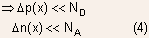
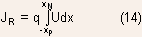
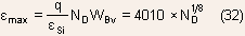
- The equation for current flowing through the diode,
derived earlier, is given by the expression:
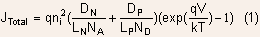
This expression was derived under the assumptions:
(i) Low Level Injection
(ii) Negligible recombination within the SCR
Although the equation was derived in the context of forward bias,
much of the derivation remains valid in reverse bias also
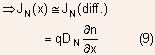
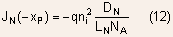
- In reverse bias, instead of injection of minority
carriers in P and N-regions, there is extraction of minority carriers
from them.
Holes now flow from  and
electrons from and
electrons from  .
.
- As a result, N-region gets depleted of holes and
P-region gets depleted of electrons
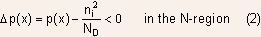
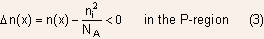
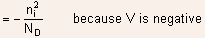
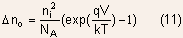
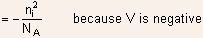
Since  can have a maximum value of
  and respectively,
These are the conditions for low level injection
if "injection" is interpreted as having a negative value
in this case
Similarly, for the N-side
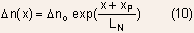
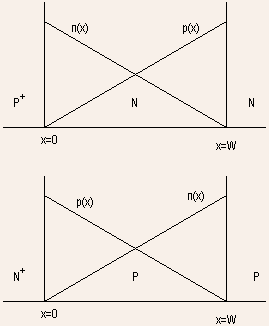
The spatial variation of electron and hole density is shown below:
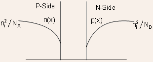
- The electrons diffuse from the bulk of the P-region
to the edge of the depletion region after which they are swept away
by the junction field. Similarly, the holes diffuse from the bulk
of the N-region to the depletion region edge after which they are
swept by the electric field to the P-region.
- The source of electrons in P-region and holes in
N-region is thermal generation of carriers.
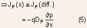
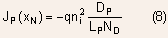
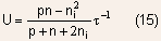
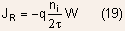
It was shown earlier, in the context of forward bias, that :

- This expression is equally valid in reverse bias
also, with the difference that the last term now represents generation
of carriers within the space charge region, instead of recombination.
- In Forward bias, we had neglected this term but as
we shall see, this term is the dominant term under reverse bias for
Silicon PN junction diodes.
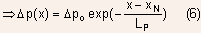
Since  within the space charge region:
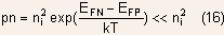
The negative sign indicates generation !
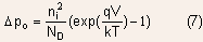
- Over a large fraction of the depletion width, the
electron and hole densities are much smaller than the intrinsic carrier
density so that
Approximation: 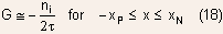
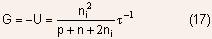
This allows the generation current to be written as :
The net reverse bias current can be written as:
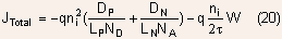
The first tem represents the current due to minority carrier diffusion
and the second due to generation within the space charge region.
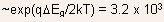
Example 3.1 Calculate the reverse leakage current for a Silicon
PN Junction with

Solution : 
For the reverse bias of 1 Volts, depletion width W=0.26µm
The magnitude of the diffusion current is 
The magnitude of the generation current is 
The generation current is several orders of magnitude larger than
the diffusion current !
The above example shows that for silicon PN junction diodes,
Because the depletion width varies as  ,
the reverse bias current would increase slowly with increase in the
reverse bias. ,
the reverse bias current would increase slowly with increase in the
reverse bias.
Example 3.2 In example 3.1 suppose a similar PN junction is
made but on a semiconductor with a bandgap of 0.7 eV. Other things
remaining the same, will it still be true that the reverse leakage
current is dominated by generation current within the depletion region?
Solution : The generation current would increase by a factor
 , while the ideal diode saturation current would increase by a factor
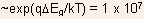 . The two currents are now comparable. For even smaller bandgaps,
the reverse leakage current will be determined entirely by the ideal
diode saturation current.
. The two currents are now comparable. For even smaller bandgaps,
the reverse leakage current will be determined entirely by the ideal
diode saturation current.
Breakdown:
- The reverse current increases slowly with increase
in reverse bias till impact ionization induced breakdown begins to
occur within the space charge region.
Impact Ionization: An electron or a hole travelling through
a region of high electric field can acquire enough energy to create
another electron-hole pair.
Impact ionization is characterized by a parameter called ionization
coefficient:
 = probability that an electron causes an impact ionization within
dx
= probability that an electron causes an impact ionization within
dx
 = probability that a hole causes an impact ionization within dx
- It is natural to expect that the ionization coefficients
would a function of carrier energy and therefore the electric field.
There are a variety of models for impact ionization coefficient, simplest
of which is :
 for Silicon (22)
- As the reverse bias increases, the electric field
within the junction also increases thereby increasing the probability
of impact ionization.
- An electron or hole generated due to impact ionization
within the depletion region can acquire enough energy again to cause
another impact ionization. The new electron-hole pairs generated can
in turn generate further electron-hole pairs.
- As a result of this process, a single carrier entering
the depletion region can get multiplied many times over. This process
of multiplication is known as Avalanche Multiplication.
- The normal reverse current gets multiplied by the
avalanche multiplication process. When avalanche multiplication becomes
large, very large reverse current begins to flow and breakdown is
said to occur.
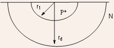
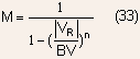
- To obtain an expression for breakdown voltage, it
has to be precisely defined. This is explained using the Figure below:
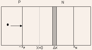
Suppose a single electron enters the depletion region at  .
Due to avalanche multiplication, .
Due to avalanche multiplication,  ,
number of electrons will come out at the end ,
number of electrons will come out at the end  .
.
Breakdown : 
- The number of electrons generated within
 will come from impact ionization caused by the electrons and holes
in this region so that
will come from impact ionization caused by the electrons and holes
in this region so that

where n(x) is the number of electrons at x travelling right to the
N-region and p(x) is the number of holes travelling left towards the
P-region.
- Since no holes are assumed to enter the depletion region, p(x) must
be due to impact ionization in the region
 . .
An equal number of electrons also must have been generated also so
that, the number of electrons that would come out of the depletion
region must be:
This allows Eq. (24) to be re-written as:
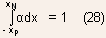
On Integrating across the depletion region:
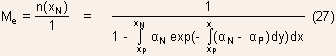
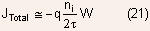
The breakdown condition for  can be now written as:
where 
The computation of breakdown voltage is simpler if we take a one sided
junction such as a P+N junction.
For this case:
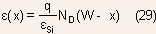
At breakdown:
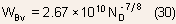
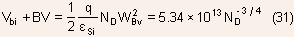
The Maximum electric field at the junction when breakdown occurs can
be expressed as:
The max. electric field at breakdown is a weak function of doping:


- It can therefore be said that whenever the maximum electric field
at the junction acquires a critical value of
 , breakdown would occur.
 Taking Taking
 at breakdown allows an estimate of the breakdown voltage to be determined
rapidly for any PN junction diode.
at breakdown allows an estimate of the breakdown voltage to be determined
rapidly for any PN junction diode.
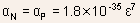
Example 2.3 Determine breakdown voltage for a PN junction shown
below Assume that  = 0.9 Volts
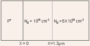
Solution : We first perform a check whether at breakdown, the
depletion width still lies in the lightly doped region or not. If
it does then, This shows that depletion width will extend into the higher doped
N-region as well resulting in the following diagram.
This shows that depletion width will extend into the higher doped
N-region as well resulting in the following diagram.
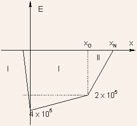
The electric field at  is obtained using the expression
 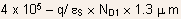 . .
Using the Poisson's equation:  .
.
The area under the electric field curve will be equal to
+ BV so that BV = 40.7 Volts .
Example 2.4 Keeping in mind that electron ionization coefficient
is larger than hole ionization coefficient , which diode  or
or  is likely to have a higher breakdown voltage with identical doping
values.
is likely to have a higher breakdown voltage with identical doping
values.
Solution : The question can be answered by examining the electron
and hole density profiles within the depletion region generated due
to impact ionization. These are shown below:
In the
junction, the electron density is maximum near the high field region
at the junction and hole density is minimum. As a result most of impact
ionization is done by electrons, while the reverse holds true for
junction. Therefore junction
will have lower breakdown voltage.
Example 2.5 Obtain an expression for the breakdown voltage
of a cylindrical PN junction. This is of interest because
junctions have a curvature near the periphery which can be considered
as cylindrical.
Solution : The Figure below shows the junction.
The Poisson equation in cylindrical coordinates can be written as
Integration of Poisson's equation with the boundary condition that
electric field at the depletion edge is zero  we obtain
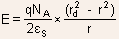
Further integration gives
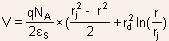
The expressions above can be used to find the breakdown voltage by
using the fact that at breakdown, the electric field is equal to the
critical field. The table below shows the breakdown voltages computed
for a doping of  and different radii of curvature.
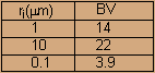
As a comparison, the breakdown voltage for a planar junction turns
out to be 31 Volts.
The expression for multiplication factor derived earlier suggests
that multiplication can be empirically modeled as
The parameter n varies with the structure of the PN junction, with
n=6 for
diode
n=4 for diode
- The avalanche breakdown is the most common mechanism of breakdown
in PN junction diodes.
- There is another mechanism called Zener breakdown that comes into
play in diodes with heavily doped P and N regions.
- As noted earlier, in reverse bias, the holes are required to flow
from the P-side to the N-side and electrons from P-side to the N-side.
The reverse current is normally small because there are so few holes
in N-region and electrons in P-region.
- However, there are plenty of electrons in valence band of P-side
and plenty of empty states in the conduction band of N-side. Except
via tunneling, the electrons from the valence band of P-region cannot
flow to empty states in the conduction band of N-side due to presence
of a potential barrier
- When the probability of tunneling becomes significant, large reverse
current begins to flow and Zener breakdown is said to occur.
The Figure below depicts the tunneling process:
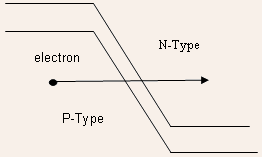
The barrier that the electron sees while tunneling, can be approximated
as a triangular barrier as shown below:
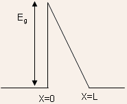
The tunneling property can be written as
Use of the triangular barrier approximation gives :
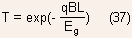
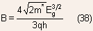
As expected, the transmission probability increases exponentially
with the thickness of the barrier which can be expressed as

where  is
the electric field within the junction. is
the electric field within the junction.
- As doping increases, the electric field increases causing barrier
to become narrower and tunneling probability to increase.
- To achieve significant tunneling, the barrier width should be only
a few tens of Angstroms.

- The field calculated for Avalanche breakdown was
 , which is lower than that required for Zener breakdown. It appears,
therefore, that avalanche breakdown would always precede Zener breakdown
!
, which is lower than that required for Zener breakdown. It appears,
therefore, that avalanche breakdown would always precede Zener breakdown
!
- However, it is not the electric field but the carrier energy that
is really important for impact ionization. A very high electric field
in a very narrow region may not allow a carrier to gain enough energy
so that impact ionization becomes significant.
- As a result, Zener breakdown occurs in very heavily doped junctions
only with small depletion widths. Because of the small depletion widths,
the breakdown voltage, despite the high electric field, is often
 Volts.
- Diodes which have breakdown voltages larger than 7-8 Volts break
down due to Avalanche multiplication process. In the intermediate
range both the processes may be active.
- It is possible to determine the breakdown mechanism by measuring
the temperature sensitivity of the breakdown voltage. Diodes which
break down via avalanche multiplication have a positive temperature
coefficient, while those that breakdown via tunneling have a negative
temperature coefficient.
- The increase in avalanche breakdown voltage with temperature occurs
due to increased scattering which makes it more difficult for carriers
to acquire energy from the electric field.
- The decrease of Zener breakdown voltage with increase in temperature
occurs because of increased carrier velocity which increases the flux
of carriers attempting to cross the barrier. Since transmission probability
remains unchanged, the tunneling current increases with temperature.
- Most of the diodes that go under the name Zener diodes have a breakdown
via avalanche multiplication rather than tunneling.
|