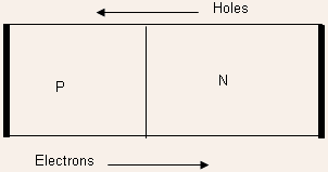
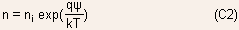
- A PN Junction is said to be in Forward Bias when the P-type region
(Anode) is made positive with respect to the N-type region (Cathode).
- A PN Junction is said to be in Reverse Bias when the P-type region
(Anode) is made negative with respect to the N-type region (Cathode).
Let us consider the Forward bias first and examine qualitatively the
mode of operation
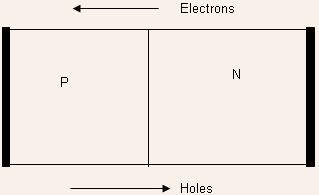
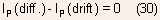
The holes are required to move from  and electrons from
  . .
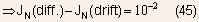
- There are plenty of holes in P-type region and would like to move
to N-region via diffusion but are prevented by the electric field
(or the energy barrier) at equilibrium. The drift and diffusion currents
cancel each other
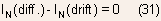
- Similarly, there are plenty of electrons in N-type region and would
like to move to P-region via diffusion but are prevented by the electric
field (or the energy barrier) at equilibrium. The drift and diffusion
currents again cancel each other.
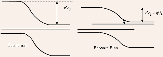
- The application of forward bias reduces the barrier and the electric
field allowing significant electron and hole current to flow:
- The fraction of electrons that are able to cross over to the P-side
or the fraction of holes that are able to cross over to the N-side
and contribute to current goes exponentially with the barrier height
(remember,
 ) )
 Current
increases exponentially with the applied forward bias. Current
increases exponentially with the applied forward bias.
Reverse Bias:
- The holes are now required by the applied bias to move from and
electrons from as
shown below:
- Although the electric field favors the flow of holes to the P-region,
there are very few holes in N-region to begin with! The number of
holes in N-region is
 , a very small number.
- Further, the number of holes is fixed and unaffected by the bias.
- Similarly, the number of available electrons in P-region for current
flow is very small and unaffected by the applied bias.
- The only thing that the applied reverse bias does is to increase
the junction electric field or the barrier height as shown below
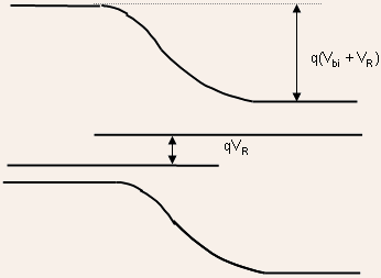
The increased electric field does not alter the current flow because
the bottleneck is the small number of carriers available for current
conduction.
Current
in Reverse bias is very small and almost constant
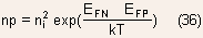
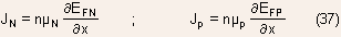
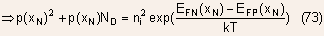
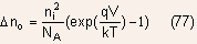
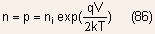
Static I-V Characteristics:
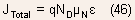
The dc current-voltage characteristics of the PN junction diode will
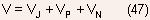
be obtained using the semiconductor equations listed below:

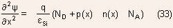
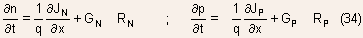

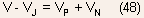
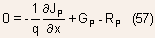
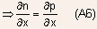
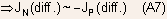
In steady state, the continuity equation reduces to
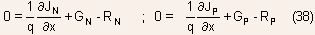
- Since for every electron lost/generated due to recombination/generation,
there is a corresponding hole lost/generated also
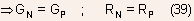
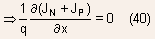

In other words, the net current flowing through the device is the
same everywhere.
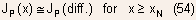
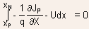
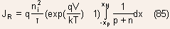
- Since the current is the same everywhere, one can choose the region
within the device for calculation of current-voltage characteristics.
Big Question : Where in the device should the current be calculated
such that its computation besides being easy is also accurate ?
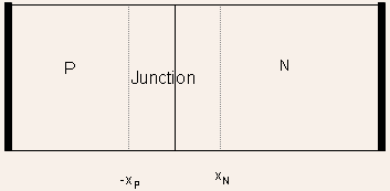
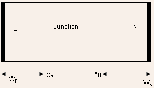
- Let us consider some alternatives: (i) At the junction:
- To appreciate the ease or difficulty of carrying out the computation
in this case, let us consider a symmetric junction with
The net electron current is equal to: 
The drift and diffusion currents oppose each other so that
Let us try to estimate the magnitude of the drift component:
- Because of symmetry n(0) = p(0) at the junction
Further : 
Assumption (i) : All the voltage is dropped across the junction:
 with the junction
Net voltage across the junction =
Assumption (ii) : Depletion approximation
- For a forward bias of 0.6V, the electron drift current can be calculated
using the results obtained as equal to

- As we shall see later, the net electron current flowing through
the junction for this device at a forward bias of 0.6V is

Because the drift current()
is five orders of magnitude larger than the net current, the drift
and diffusion currents would have to be calculated to an accuracy
of .001% to obtain a correct estimate of the net electron current!
This
makes the estimation of total current via an analysis at the junction
virtually impossible!
- Let us consider a region for estimation of current which is far
from the junction in say N-type semiconductor.
- Far from the junction, on the N-side, the current is expected to
be primarily an electron current. Any holes which are injected from
the P-side would recombine and disappear away from the junction.
- The electron density being constant, the electron current would
be primarily a drift current so that
It might appear that this is a very good place for estimation of current
because we have just one component and only one unknown , the electric
field .
- However, this electric field is extremely difficult to estimate
because of its very small value.
The voltage applied across the diode gets dropped partially across
the junction and partially outside it
where the last two terms represent the voltage dropped across the
neutral N and P-regions
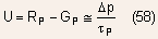
- The bottleneck for current flow in a PN junction is the space charge
region where the potential barrier exists. As a result,
 is
almost equal to the applied voltage is
almost equal to the applied voltage
While it is easy to compute the junction voltage fairly accurately,
the estimation of residual drops in the neutral regions becomes very
difficult.
- The two examples discussed earlier illustrate that the choice of
position in the PN junction for computation of its I-V characteristics
is very important.
- As first demonstrated by Shockley, the computation of currents in
PN junction diode is best done at the edges of depletion region as
explained below:


- During the course of the analysis, several assumptions will be made.
There are two ways of justifying these assumptions. One of them is:
(i) Make the assumption
(ii) Solve the resulting simplified equations to obtain the current-voltage
characteristics
(iii) Check that the assumptions made are consistent with the results
obtained.
The assumptions made will be consistent only for certain range of
currents, so that the range of validity of the model will be obtained.
- The other approach is to justify the assumptions in the beginning
of the analysis, based on available device characteristics. These
assumptions would define the range of validity of the obtained model.
We shall follow a mix of these two approaches
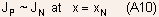
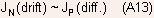
Assumption (1): Negligible recombination within the Junction
We shall justify this assumption using the first approach, namely
that the assumption would be shown to be consistent with the results
obtained within certain limits.
All
the ho;es that are injected at  reach
the point reach
the point  so that
Similarly all the electrons that are injected at reach
the point
, so that
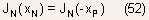
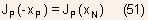
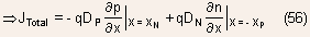
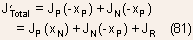
This allows the total current to be expressed as :
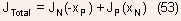
The
total current can be computed by computing the minority carrier currents
at the edges of depletion region in N and P-regions
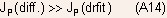
Assumption (2) : Minority carrier current is largely diffusive
We shall justify this assumption using the second approach, namely
that the validity of this assumption will be demonstrated prior to
analysis. This is described in Appendix A.
The assumption implies :

The
task of computing the currents boils down to the computation of minority
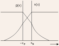
carrier profiles: p(x) in N-region and n(x) in P-region.
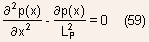
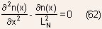
- The minority carrier profile can be determined by solving the continuity
equation with appropriate boundary conditions
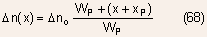
For hole density in N-region:
- In Silicon, the dominant recombination mechanism is the Shockley-Hall-Read
recombination which can be described by the relation
under low level injection conditions.  is the hole recombination lifetime in N-type material.
The hole continuity equation can be re-written as
where  has the units of length and as we shall see later is appropriately
called the hole diffusion length
has the units of length and as we shall see later is appropriately
called the hole diffusion length
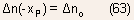
Boundary Conditions:
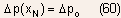
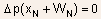 assuming ideal ohmic contact .
Solution:
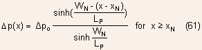
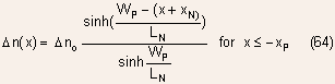
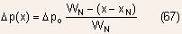
Similarly for the N-side:
where  is called the electron diffusion length.
Boundary conditions:
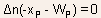 assuming ideal ohmic contact
There are two extreme cases:
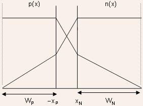
(i) Wide Base diode: 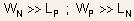
For this case, the minority carrier densities can be simplified to:
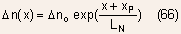
The
minority carrier densities decay exponentially with the distance from
the junction, with a characteristics decay length of  for
holes and for
holes and  for electrons.
- It can be shown that the average distance a hole diffuses before
recombining is equal to so
that it is called the diffusion length.
The other extreme case is :
(ii) Narrow Base diode: 
The minority carrier profile can be simplified to
The carrier densities vary linearly with position now !
- The total diode current for wide and narrow base diodes can be expressed
as
Wide base diode:
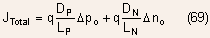
Narrow base diode:
The
task of determining the I-V Characteristics now reduces to finding
a relationship between the minority carrier densities at the edges
of depletion region and the applied voltage.
We start with the relation:
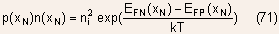
where quasi-neutrality 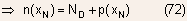
The low level injection assumption invoked earlier can be used here
also for simplification. The first obvious consequence is that

So that the first term on the LHS of the above expression can be neglected.
The second consequence of low level injection, explained in detail
in Appendix A is that
 for
for  in the N-region and the depletion region
-
 for
for  in the P-region and the depletion region
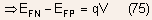
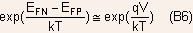
- The quasi-Fermi level
 on the N-side must coincide with the Fermi level of the metal forming
the ohmic contact to the N-side if an ideal contact with no voltage
drop across it is assumed.
on the N-side must coincide with the Fermi level of the metal forming
the ohmic contact to the N-side if an ideal contact with no voltage
drop across it is assumed.
- Similarly, the quasi-Fermi level
 on the P-side must coincide with the Fermi level of the metal forming
the ohmic contact to the P-side if an ideal contact with no voltage
drop across it is assumed.
on the P-side must coincide with the Fermi level of the metal forming
the ohmic contact to the P-side if an ideal contact with no voltage
drop across it is assumed.
Since a voltage V is applied between the two ohmic contacts:
This allows the minority carrier densities at the edges of depletion
region to be expressed as
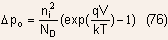
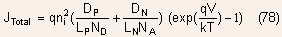
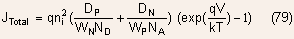
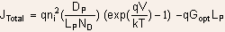
- The total current density for the diode at a bias of V volts can
now be expressed as
Wide base diode:
Narrow base diode:
- The current varies exponentially with applied voltage when the diode
is forward biased (V > 0)
- The current is constant and small when the diode is reverse biased
(V < 0)
Example 2.1 A uniformly doped Silicon PN junction with very
thick P and N regions has the following characteristics:
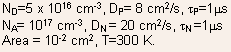
For a forward bias of 0.626 Volts, calculate, excess minority carrier
concentrations and minority carrier currents at the edges of depletion
region. Calculate also the net current flowing through the device.
Solution : The wide-base diode is model valid here. Using the
expressions derived earlier:
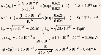
The net current is the sum of electron and hole current = 0.56+0.44
= 1 mA.
Example 2.2 For the example above, determine expressions for
(a) majority carrier currents in N and P-regions
(b) majority carrier diffusion currents in N and P regions
(c) majority carrier drift currents in N and P regions
(d) electric field in the N-region
(e) minority carrier drift currents. Confirm that they are much smaller
than minority carrier diffusion currents calculated in example 2.1
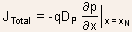
Solution: We will carry out the solution for the N-region since
the solution for P-region is similar. The minority hole current in
N-region can be written using the results of previous example as:
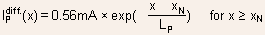
The hole current is primarily diffusion current and the sum of hole
and electron currents is equal to the total current. The electron
current on the N-side is therefore simply:
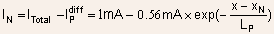
The electron diffusion current can be written as:

Using the concept of quasi-neutrality in the N-region : =.gif) ,
so that ,
so that

The electron diffusion current can therefore be expressed as
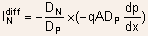
The term in the bracket is simply the hole diffusion current which
has already been obtained earlier:
The electron drift current can be written as
The low level injection assumption holds true in this case because
 so that
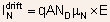
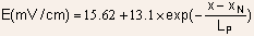
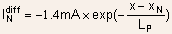
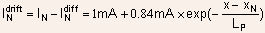
An electron mobility of 800  was assumed. Let us calculate the hole drift current at the depletion
edge where there is an electric field of 28.7 mV/cm. The hole drift
current is
was assumed. Let us calculate the hole drift current at the depletion
edge where there is an electric field of 28.7 mV/cm. The hole drift
current is

which is much smaller than the diffusion current component.
Example 2.3 A PN junction diode has the same characteristics
as that of example 2.1 except that the thickness of the N region  The thickness of the P-region remains very long. Calculate the total
current flowing through the diode.
The thickness of the P-region remains very long. Calculate the total
current flowing through the diode.
Solution : This is an example of a diode that can neither be
considered a fully wide-base
diode nor a fully narrow-base diode. On the P-side, the diode is very
thick so that we can
use the expression for electron current valid for wide base diodes.
Therefore
 as before.
On the N-side  so that the narrow-base model can be used
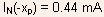
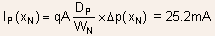
The net current will be 0.44 + 25.2 mA = 25.64 mA.
The current is predominantly determined by the narrow base side of
the junction.
Example 2.4 Suppose the P-side thickness is also reduced to
 .
Calculate the total current flowing through the diode again. .
Calculate the total current flowing through the diode again.
Solution: This diode can be modeled as a narrow-base diode. We
have already calculated the hole current in example 2.3 which remains
the same. The electron can similarly be calculated as
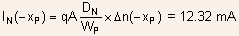
The net current will be 12.32+25.2 = 37.5 mA
This current is significantly higher than that calculated for wide-base
diode in
example 2.1. This illustrates that for comparable doping values, narrow-base
diodes provide higher current for the same bias or equivalently have
a smaller turn-on voltage.
The expression for current was derived on the basis of two assumptions:
(i) negligible recombination within the depletion region
(ii) low level injection within N and P-regions
These assumptions limit the range of validity of the derived expression.
The first assumption determines the lower limit, while the second
assumption determines the upper limit.
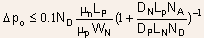
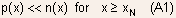
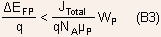
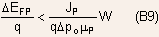
Lower limit: As stated earlier, this is determined by neglect of space
charge recombination.
If the hole continuity equation is integrated across the depletion
region, we obtain the relation
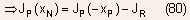
where 
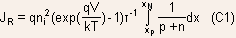
Eq.(80) implies that the correct expression for total current should
be
In other words
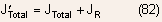
So as long as  , the neglect of SCR recombination is justified
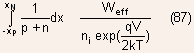
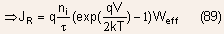
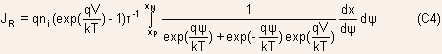
- So what we need to do first is to get an estimate for the SCR recombination
current:
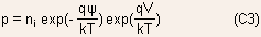
We shall use a simple model for the Shockley-Hall-Read recombination:
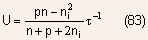
The recombination is assumed to take place via a single deep level
at the midgap with equal hole and electron recombination lifetimes
Within the depletion region:

where the definition  has been used
Noting that either p(x) or  : :
- Because of the exponential dependence of p and n on the voltage
(which varies quadratically with x ), the function
 is a rapidly varying function of the form shown below:
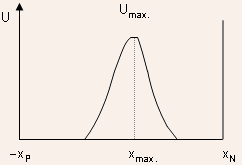
The recombination rate would have a peak value where the factor
attains a maximum value. Since pn = constant,this would occur
when
The sharp variation of U implies that most of the recombination current
comes from a small region around the peak value. This allows the following
simplification to be performed:
In appendix C, this relation is derived more rigorously, where it
is also shown that
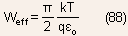
where  is the magnitude of the electric field at the place where peak recombination
occurs.
is the magnitude of the electric field at the place where peak recombination
occurs.
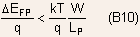
Let us now determine the condition under which
Substituting the expressions for  and
and  derived earlier, we obtain the following condition:
So as long as

recombination within the SCR can be neglected within ~10% accuracy
and the ideal diode equation can be used.
- For values of current
 ,
the diode current would be determined primarily by the SCR recombination
current. ,
the diode current would be determined primarily by the SCR recombination
current.
If we compare this recombination current with ideal diode current,
we can see two major differences:
(i) The ideal diode current increases as  while the recombination current increases as
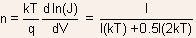
The other way of stating this is that the ideality factor defined
as
is unity for ideal diode current and 2 for SCR recombination current.
(ii) The SCR current goes as  , while the ideal current goes as
  for
wide base diode and is independent of lifetime for narrow base diodes. for
wide base diode and is independent of lifetime for narrow base diodes.
It
is for this reason that the SCR current is considered as an index
of material quality because the recombination lifetime is very sensitive
to fabrication conditions.
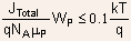
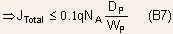
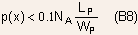
- The upper limit for the validity of ideal diode equation is determined
by the assumption of low level injection condition.
This low level injection condition will first break down for the region
which has the smaller doping level. We shall assume, for the sake
of discussion, that N-region is the lightly doped region.
- The low level injection assumption had allowed the following simplifications
to be made:
(i) Minority carrier current is diffusive
(ii) The expression 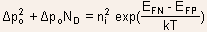 to be simplified as
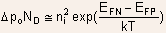
(iii) 
- The major departure in I-V Characteristics is caused by the breakdown
of (ii) and (iii) relations because they are associated with an exponential
factor.
When  , the actual minority carrier density at the depletion edge is about
10 % smaller than that predicted by the simplified expression.
, the actual minority carrier density at the depletion edge is about
10 % smaller than that predicted by the simplified expression.
- The (iii) simplification amounted to neglect of the IR drop in the
N-region. This drop is negligible when
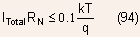
The expression for current under these conditions remains valid so
that
 for wide base diode
 for wide base diode
All these limits are comparable in nature so that for  ,
the ideal diode equation ca be assumed to be valid. ,
the ideal diode equation ca be assumed to be valid.
The upper limit for the validity of the ideal equation is then:
 for wide base diode (95)
 for wide base diode (96)
So for  , the ideal diode equation remains valid.
Example 2.5 Calculate the range of validity for ideal diode
equation for a wide base diode described in Example 2.1.
Solution : For simplicity, we take
in Eq. (88) to be  at V=0.6Volts

For this example, the ideal diode equation is valid over five orders
of magnitude variation of current. It is because of the wide range
of validity of the final equation, that the assumptions of negligible
SCR recombination and low level injection are such good assumptions!
Example 2.6 For a forward bias of 0.326 Volts, calculate the ideality
factor of the current for a PN junction described in Example 2.1
Solution : In general, the current consists of two components;
one kT-like ideal diode current with ideality factor 1 and another
2kT-like space charge generation/recombination current with ideality
factor 2:

Using Eq. (78) and Eq. (89) we obtain I(kT) = 10 nA and I(2kT) = 11
nA
n = 1.35
Example 2.7 Determine expression for current in a wide-base  junction illuminated with light. For simplicity assume that there
is a uniform carrier generation rate
junction illuminated with light. For simplicity assume that there
is a uniform carrier generation rate  .
.
Solution : For a
diode, the current would be determined primarily by hole injection
into the N-region so that under low level injection conditions:
The hole continuity equation now includes an additional term due to
optical generation rate:
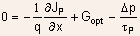
The hole continuity equation can be re-written as
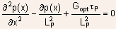
The solution of this equation gives: 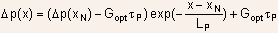
As before: 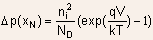
The net current can be written as:
Thus the current includes an additional component due to light which
represents the current due to flow of carriers generated effectively
within a distance of one diffusion length of the depletion edge. There
would be an optical generation current due to generation within the
depletion region as well which can be written as  ,
where W is the total depletion width. Since depletion width is often
much smaller than diffusion length, this component can be neglected.
However, in some especially designed PIN diode structures, this component
is the dominant current. ,
where W is the total depletion width. Since depletion width is often
much smaller than diffusion length, this component can be neglected.
However, in some especially designed PIN diode structures, this component
is the dominant current.
Example 2.8 In the analysis of narrow base diodes, it was assumed
that the excess carrier density at the contact is zero. This however
is true only if the contact can be assumed to be ideal. For practical
contacts, the excess carrier density may be small but is nonzero.
These contacts are characterized by a parameter called surface recombination
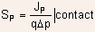
velocity, which for holes can be defined as
(a) Derive an expression for current in a
diode using the above boundary condition
(b) Determine the value of SP that is needed for a contact to be considered
ideal.
Assume a diode with 
Solution : 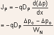
Using the boundary condition at the contact:  , we obtain the final expression for current:
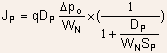 s
s
(b) The first term represents the standard current expression, while
the second term represents the modification due to finite recombination
velocity. The equation above shows that as  , the expression becomes identical with that derived for ideal contacts.
Thus an ideal contact is one with an infinite recombination velocity.
More
, the expression becomes identical with that derived for ideal contacts.
Thus an ideal contact is one with an infinite recombination velocity.
More
practically when the factor  , then the contact could be considered almost
ideal. This condition for the values given translates into 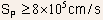 .
.
Appendix A
- The assumption that minority carrier current is largely diffusive
can be shown to be true provided low level injection conditions prevail
within the device:
Consequences of Low Level Injection:
In the N-region: 
In the P-region: 
We will need another result before we can demonstrate the soundness
of our assumption: The regions outside the space charge region are
quasi-neutral so that:
In the N-region: 
Similarly,
In the P-region: 

- We will now show that the minority carrier currents can be assumed
to be diffusive provided low level injection condition prevails. Although
this result is general, we shall assume that the N and P regions are
of comparable doping. This implies that the electron and hole currents
close to the depletion edge will also be comparable.


We have already shown that electron and hole diffusion currents are
comparable and that for low level injection electron drift current
is much larger than the hole drift current in the N-region so that
Appendix B
- To show that
 in the P-region and within the depletion region.
Similarly,  in the N-region and within the depletion region.
We shall first consider the neutral P-region and show that for low
level injection conditions, the hole quasi Fermi level can be considered
to be almost flat.
We start with the expression: 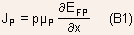
Noting that  : :
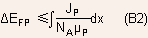
where the integral is over the entire length of the neutral P-region.
Since 
Noting that the resistance of the neutral p-region is
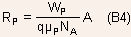
where A is the device crossectional area, we can obtain
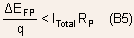
Therefore, as long as the IR drop is sufficiently small, the hole
quasi-Fermi level can be assumed to be constant.
How much is sufficiently small ?
As shown in the main text, the expression which results from making
the assumption is
Therefore, as long as  ,
the error will be less than 10%. ,
the error will be less than 10%.
What is this constraint in terms of injection level?
Since 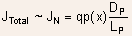 we obtain the constraint:
This constraint would be satisfied if  : the low level injection condition!
- That hole and electron quasi-Fermi levels can be assumed to be flat
within the depletion region can be demonstrated as follows:
As before, we start with the expression: 
Noting that within the depletion region

where W is the depletion width
Since, 
We obtain
So as long as  , The assumption is fine
- Since the depletion width is of the order
 and diffusion length
  , the assumption is very well satisfied.
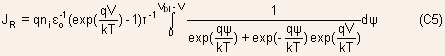
Appendix C
Substitution of the expressions for electron and hole densities in
the expression for current results in
Since most of the recombination occurs within a very narrow spatial
region and electric field is a slowly varying function, it can be
taken out of the integral with a value at the position of maximum
recombination rate ().
Substitution of  in the above expression allows the integral to be re-written
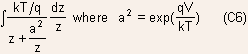
The limits of integration correspond to  and
and  .
Upon Integration , one obtains .
Upon Integration , one obtains
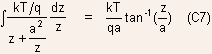
Substitution of the limits of integration gives
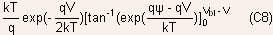
Using the approximation that  , we obtain the final expression for the integral as
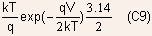
The required expression for current can now be obtained by substituting
this expression in Eq. (C5)
|