- PN junctions are important for the following reasons:
(i) PN junction is an important semiconductor device in itself and
used in a wide variety of applications such as rectifiers, Photodetectors,
light emitting diodes and lasers etc
(ii) PN junctions are an integral part of other important semiconductor
devices such as BJTs, JFETS and MOSFETs
(iii) PN junctions are used as test structures for measuring important
semiconductor properties such as doping, defect density, lifetime
etc
- The discussion associated with the PN junctions will proceed in
the following order:
(i) PN junction in equilibrium
(ii) dc IV characteristics in forward bias
(iii) characteristics in reverse bias
(iv) dynamic characteristics
(v) Circuit models
(vi) Design perspective
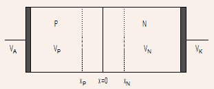
Device Structure :
The Figure below shows a simplified structure of a PN junction:
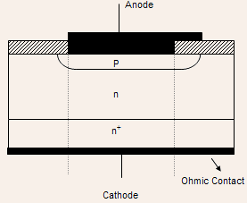
- The structure can be fabricated by diffusing P-type impurity in
the n-epilayer grown over an
 substrate. substrate.
- While the doping in the n-epilayer can be uniform, the doping in
the P-region is often either Gaussian or error-function in nature.
The doping profiles and the junction are schematically illustrated
below:
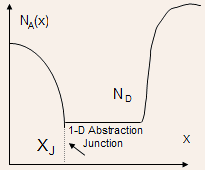
1-D Abstraction
- Even though the doping in both N and P-regions may in general be
nonuniform, for simplicity, we shall assume them to be uniform in
the initial analysis because the basic device physics remains almost
the same
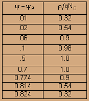
- A simplified, one-dimensional abstracted view of a PN junction described
by the region within the dotted lines of device schematic is shown
below:
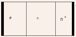
- We shall assume that the thicknesses of P and N-regions are large
enough so that one can ignore the presence of Ohmic contacts and the
heavily doped N-region and consider only the P and N regions for analysis.
Such a diode with wide N and P-regions is called a wide-base diode.
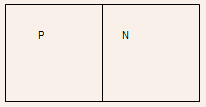
- The PN junction that we shall study will therefore be a 1-D structure
with uniformly doped P and N regions with thicknesses sufficiently
large to ignore effects of contacts and other layers. It shall be
represented simply as
PN junction in Equilibrium
- As mentioned earlier, the characteristics of a semiconductor device
is completely specified in equilibrium if the variation of potential
as a function of position is specified. As a first step to obtaining
this potential profile, we shall sketch the energy-band diagram of
the device. The energy band diagram would provide us with
(i) a qualitative variation of potential in the device
(ii) boundary conditions for solution of Poisson's equation
-
As usual, the energy band diagram of the PN junction
will be obtained by combining the energy band diagrams of N and
P-type semiconductors separately
Energy Band Diagram In Equilibrium
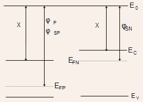
Energy Band diagram of N- and P-regions before equilibrium
- When the N and P-regions are brought into contact, the electrons
would flow from regions of higher Fermi-energy to regions of lower
Fermi energy and holes would flow in the opposite direction.
- Because of loss of electrons, the N-region would acquire a net positive
charge due to the uncovered positively charged donor atoms and P-region
would acquire a negative charge due to uncovered negatively charged
acceptor atoms.
- At equilibrium there is no net flow of either electrons or holes
so that the PN junction has a single constant Fermi level.
- The transfer of charges will affect only the regions close to the
junction so that regions which are far still have the same energy
band diagram(i.e. same relative positions of conduction and valence
band wrt Fermi energy)
- As we approach the junction from the N-side, the conduction band
must bend upwards away from the Fermi energy to indicate the fact
that the region is progressively getting depleted of electrons ( remember
 . .
- Similarly, as we approach the junction from the P-side, the conduction
band must bend downwards towards the Fermi energy to indicate the
fact that the region is getting depleted of holes
Using these principles, the final energy band diagram can be sketched
as
- As a result of transfer of charges from N and P-regions, the region
next to the junction is charged and is known as the space charge region.
- The charge on the N-side is positive and on the P-side negative.
- As a result, the space charge region will have an electric field
directed from the N to the P-region with a maximum value at the junction
and zero at the edges of the space charge region.
- As a result of the electric field, there will be a net voltage across
the space charge region known as the built-in voltage.
- The magnitude of the built-in voltage can be quickly estimated from
the energy band diagram. We do this by performing an analog of Kirchoffs
voltage law:
We start from a point in the N-region(away from the space charge region)
at the energy  and
then move to a point in the P-region(away from the space charge region)again
at energy via
any path other than the Fermi-energy and add up the energy gained
or loss at each step of the path, then the net sum should be zero! and
then move to a point in the P-region(away from the space charge region)again
at energy via
any path other than the Fermi-energy and add up the energy gained
or loss at each step of the path, then the net sum should be zero!
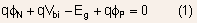
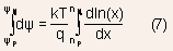
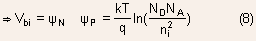
The built-in oltage can be expessed as:
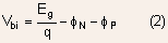
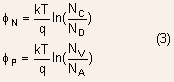
For Non-degenerate semiconductors:
- An important result that can be deduced from Eq.(2) is that built-in
voltage will be higher for semiconductors with larger bandgap.
Using the relationship 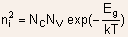 ,
the expression for built-in voltage for a ,
the expression for built-in voltage for a
PN junction having non-degenerate semiconductors can be written as
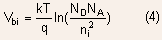
Example 1.1 Determine the built in voltage for a uniformly
doped Silicon PN junction with 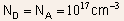 at
room temperature. Will the built-in voltage increase or decrease with
increase in temperature? at
room temperature. Will the built-in voltage increase or decrease with
increase in temperature?
Substitution of the doping values in Eq. (4) gives
The built-in voltage decreases with increase in temperature due to
exponential increase of intrinsic carrier concentration with temperature.
The pre-factor kT/q in Eq.(4) has a much lesser influence.
- There is another method by which the magnitude of built-in voltage
can be obtained. In this case we start with the fact that in equilibrium,
the net electron current is zero:
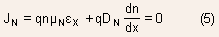
Use of Einstein's relation :  allows
the above expression to be re-written as: allows
the above expression to be re-written as:
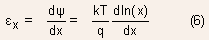
Integrating the above expression across the space charge region gives:
where  are the potentials in the bulk of N- and P- regions respectively.
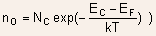
 is the electron density in the N-region and
  is the elecron density in the P-region.
Example 1.2 Can the built-in voltage of the PN junction be
measured by simply connecting a voltmeter across its two terminals?
The answer is NO and this can be explained in several ways:
- Although there is a net voltage across P and N-regions, the built-in
voltage does not appear across the external terminals. If it did,
then upon connection of a resistor across it, a current would begin
to flow. This contradicts the fact that no current can flow in equilibrium.
So how does the voltage across the external terminals become zero?
- The built-in voltage is cancelled by voltage drop across the contacts
made to N and P-regions.
The net voltage between anode and cathode terminals can be written
as

The first term on the RHS represents the contact potential or barrier
height for the Anode/P metal-semiconductor junction. Keeping in mind
that contact potential between any two materials is simply the difference
of their work-functions, we obtain
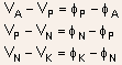
where  and are the work functions of P-type, N-type, cathode and anode metals
respectively. For simplicity we asume that both anode and cathode
metals are same ( say aluminium ) so that
and are the work functions of P-type, N-type, cathode and anode metals
respectively. For simplicity we asume that both anode and cathode
metals are same ( say aluminium ) so that  Using four equations given above, it is easy to see that
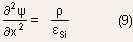
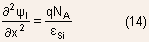
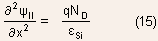
Poisson's equation
- The energy band diagram gives only a qualitative variation of potential
across the space charge region. The detailed nature of this potential
can be obtained through the solution of Poisson equation:
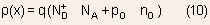
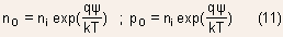
Analytical Solution of Poisson's equation
- Because of the exponential terms in the expression for charge density,
the analytical solution of the Poisson's equation becomes difficult.
- This difficulty is overcome through the assumption that the electron
and hole density within the space charge region is negligible as compared
to the ionized donor or acceptor atom density. This approximation,
known as the depletion approximation, allows the Poisson equation
to be simplified to:
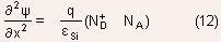
Henceforth, we shall also assume that all donor and acceptor atoms
are ionized.
- The table below shows the charge density as a function of potential
within the space charge region for a PN junction with same doping
 in N and P regions for simplicity.
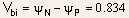
- The data in the table shows that over a large range of potential,
the depletion approximation is valid. Only for regions close to the
space charge edge, does the approximation become weak.
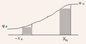
Simplified Charge density
With the depletion approximation , the charge density can be expressed
as
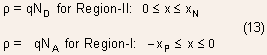
The space charge region is often called the depletion region
| Simplified
Poisson Equation |
The Poisson's equation for P and N-regions of the depletion region
can be written as
The boundary conditions can be written as:
The boundary conditions can be written as:
Outside the space region the charge density is zero so that
This implies that electric field outside the depletion region is constant.
However, to be consistent, this electric field must be zero, otherwise
it would imply a non-zero current, some applied bias etc.
- The electric field at x=0 must be continuous, otherwise it would
imply an infinite charge density.
- Similarly, the potential at x=0 also must be continuous
- The Poisson equation with these boundary conditions can be easily
solved to obtain the following results.
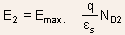
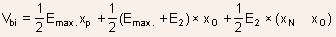
Solution:
Electric field: It is max. at the junction
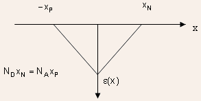
Potential:
- The variation of potential across the depletion region is parabolic.
Using the boundary condition that potential must be continuous at
the junction:
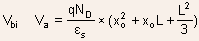
- Deletion widths: Using the relation
 ,
we can obtain ,
we can obtain
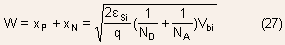
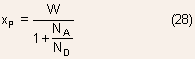
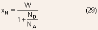
- The depletion widths vary inversely with the doping.
Example 1.3 Determine the total depletion width and the magnitude
of maximum electric field for a symmetrical Si PN junction at equilibrium
for doping densities of 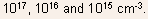
Using Eq.(23) and (27), we can obtain the following set of values
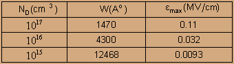
The depletion width increases with decrease in doping but the magnitude
of maximum electric field decreases even though the space charge region
gets wider. This is because while the width of the space charge region
increases as  ,
the charge density with in the space charge region decreases as ,
the charge density with in the space charge region decreases as  as
the doping is reduced. This results in a net decrease in charge and
therefore the electric field at the junction. as
the doping is reduced. This results in a net decrease in charge and
therefore the electric field at the junction.
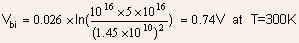
Example 1.4 Determine the built-in voltage for a Silicon PN
junction with uniformly doped P region with  and
an N-region which consists of two uniformly doped regions but of different
doping values as illustrated below. and
an N-region which consists of two uniformly doped regions but of different
doping values as illustrated below.
The difficulty in this problem is that while it is clear that in Eq.(4),
it is not clear whether the N-type doping should be
 or 5 x
 .
The answer depends on where the depletion edge in N-region lies. Let
us assume that it lies in the lightly doped region so that we take .
The answer depends on where the depletion edge in N-region lies. Let
us assume that it lies in the lightly doped region so that we take
 =.This
gives a =.This
gives a  of
0.7 volts.We have to check whether our assumption is correct or not.
Use of Eq.(27) shows that depletion width is 4257 of
0.7 volts.We have to check whether our assumption is correct or not.
Use of Eq.(27) shows that depletion width is 4257  thereby
validating our aasumption. If assumption had been wrong, we would
have to redo our calculations with =5
x . thereby
validating our aasumption. If assumption had been wrong, we would
have to redo our calculations with =5
x .
As the PN junction is reverse biased, the depletion width increases
so that eventually the depletion edge would lie in the higher doped
N-region. In that case also a new value of built-in voltage would
have to calculated and used in the expressions for depletion width,
electric field etc.
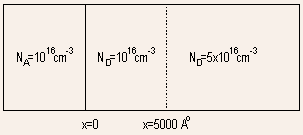
Example 1.5 Suppose in the example above, the thickness of
the lightly doped region is 2500 only.
Calculate the depletion width at equilibrium.
Using the previous example, we know that the depletion edge will lie
in the higher doped N-region so that
To find the depletion widths , we can adopt the methodology used for
uniformly doped PN junctions except that solution of Poisson's equation
is carried out in three regions, with region I being P-type , region
II being N-type with doping  and
region III with N-type doping of and
region III with N-type doping of  The boundary conditions are similar except that two new boundary conditions
describing continuity of potential and electric field will have to
be used at the boundary of regions II and III.
The boundary conditions are similar except that two new boundary conditions
describing continuity of potential and electric field will have to
be used at the boundary of regions II and III.
An alternative to working out the solution by beginning from Poisson's
equation is to use some of the results already obtained with uniformly
doped PN junctions. For example, we know that the electric field will
vary linearly and can be sketched as
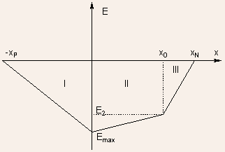
Using the concept of charge neutrality, meaning that net charge on
the P-side must be balanced by net charge on the N-side, we can write
The slopes of electric field in each region can be written straight
from Poisson equation.
For example, in region II, 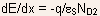 so
that so
that
and similarly using Poisson equation on the P-side in region I

In these equation  refers
only to the magnitude of the maximum electric field. The area under
the curve is simply the total voltage across the junction so that refers
only to the magnitude of the maximum electric field. The area under
the curve is simply the total voltage across the junction so that
Solution of the above equations will give values for  and
therefore the total depletion width. and
therefore the total depletion width.
| Comparison With Exact Numerical calculations |
The Figure below shows a comparison of an actual charge profile computed
using a 1-D device simulator and charge profile under depletion approximation
for a doping of  . .
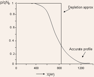
The Figure above shows that the transition region is about 600 ,
almost same as the depletion width(735 )
predicted by the depletion approximation!
- The depletion approximation therefore appears to be a poor assumption.
However, a careful look shows that the depletion assumption overestimates
the charge in region I but underestimates the charge in region II.
Since, the electric field and potential are determined by the integral
of charge density, the error in electric field and potential profile
is not large!
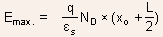
Example 1.6 Instead of approximating the charge density profile
by an abrupt transition region, a better approximation would be to
have a linear approximation to the transition region as illustrated
below for a PN junction with same value of doping in both N and P
regions.
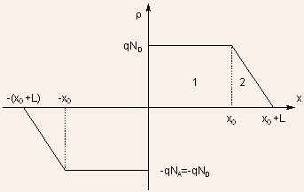
Obtain expressions for electric field and potential
Integration of Poisson's equation in regions 1 and 2 and matching
the electric field at the boundary gives
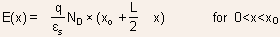

The maximum electric field is given by the expression:
Integration of electric field with the condition that the net voltage
across the space charge region is  ,
gives ,
gives
Example 1.7 So far we have discussed PN junctions in which
both P and N-regions are made out of the same semiconductor. Let us
consider next an 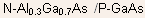 heterojunction and sketch its band diagram at equilibrium and find
its barrier height.
heterojunction and sketch its band diagram at equilibrium and find
its barrier height.
Figure below shows the band diagram of the two semiconductors, when
they are far apart.
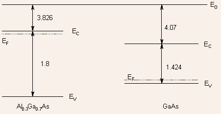
Using the principles described earlier, the band diagram after equilibrium
can be sketched as
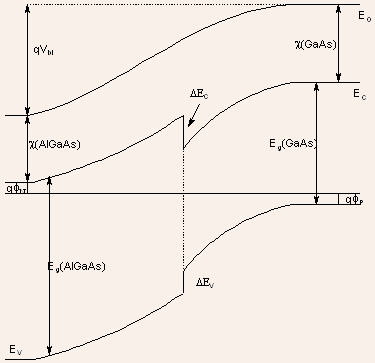
There exists a discontinuity in conduction band and valence band at
the junction. Their magnitudes can be expressed as
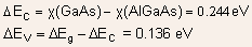
where  is
the difference in the bandgaps of the two semiconductors is
the difference in the bandgaps of the two semiconductors
The barrier height can be determined by performing an analog of Kirchoffs
law. We start from a point at Fermi energy in the P-type GaAs far
from the junction and arrive again at the Fermi energy but on the
side of N-AlGaAs, again far from the junction and add up all the energy
increments along the way:


The first term is the usual term that is present in the expression
for built-in voltages of homojunctions also. The second term is the
additional term that results from the presence of conduction-band
discontinuity.
|